Computer Organization and Architecture: Chapter 3: Processor Design
Simple Implementation Scheme and Drawbacks
Processor Design
Questions: 1. State the advantages of multiple levels of decoding. 2. Give instruction formats for R type, load or store and branch instructions. 3. Draw the simple combine datapath with all necessary multiplexers and control lines. 4. State the functions of following control lines. a) PC Src b) ALU Src c) RegDst d) Mem R 5. Draw and explain the simple datapath with the control unit and explain the execution of ALU instructions. 6. With the help of a neat diagram explain the operation of datapath for R type instruction. 7. With the help of a neat diagram explain the operation of datapath for load instruction. 8. Give the sequential steps required for execution of R‒type instruction.
Simple
Implementation Scheme and Drawbacks
•
Here, we restrict ourselves to implement load word (lw), store word (sw),
branch equal (beq), and the arithmetic‒logical instructions add, sub, AND, OR
and set on less than. We will also the design to include a jump instruction
(j).
1. The ALU Control
• The MIPS ALU defines the six following combinations of four control inputs:
ALU control lines Function
0000 ‒ AND
0001 ‒ OR
0010 ‒ Add
0110 ‒ Subtract
0111 ‒ Set on
less than
1100 ‒ NOR
•
Depending on the instruction class, the ALU will need to perform one of these
first five functions. (NOR function is needed for other parts of the MIPS
instruction set. It is not included in the subset we are implementing.)
■
In case of load word and store word instructions, we use the ALU to compute the
memory address by addition.
■
In case of the R‒type instructions, the ALU needs to perform one of the five
actions ‒ AND, OR, subtract, add or set on less than.
■
In case of branch equal, the ALU must perform a subtraction.
•
We can control the operation of ALU by the 4‒bits ALU control input and 2‒bits
ALUOp. The 2‒bits ALUOp is interpreted as shown in Table 3.4.1.
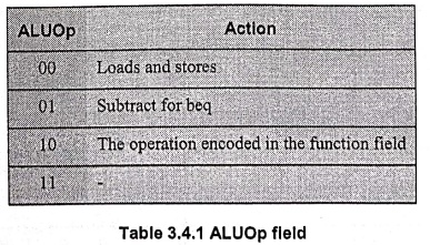
ALUOP : Action
00 : Loads
and stores
01 : Subtract
for beq
10 : The
operation encoded in the function field
11 ‒
•
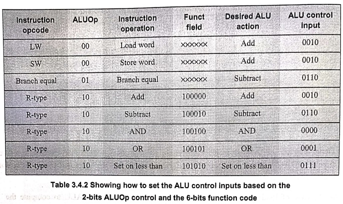
Table 3.4.2 shows how to set the ALU control inputs based on the 2‒bits ALUOP
control and the 6‒bits function code.
•
Here, multiple levels of decoding technique is used.
Advantages of using multiple levels of decoding
■
It reduces the size of the main control unit.
■
Use of several smaller control units may also potentially increase the speed of
the control unit.
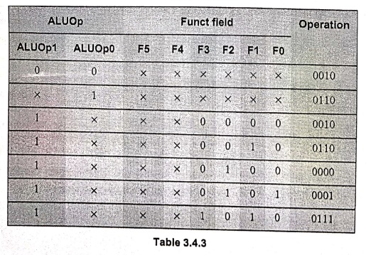
Table
3.4.3 shows how the 4‒bits ALU control is set depending on these two input
fields : function fields and 2‒bits ALUOp field.
•
Once the truth table has been constructed, it can be optimized and can be
implemented using logic gates.
2. Designing the Main Control Unit
•
Before looking at the rest of the control design, it is useful to review the
formats of the three instruction classes: The R‒type, branch and load‒store
instructions. Fig. 3.4.1 shows these formats.
• Format for R‒format
instructions: Opcode is 0. These instructions have
three register operands: rs, rt and rd. Fields rs and rt are sources and rd is
the destination. The funct (Function) field is an ALU function discussed in the
previous section. The shamt field is used only for shifts.
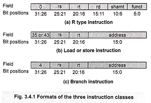
• Format for load and
store instructions: Load
(opcode = 3510) or store (opcode = 4310). The register rs
is the base register that is added to the 16‒bit address field to form the
memory address. For loads, rt is the destination register for the loaded value.
For stores, rt is the source register whose value should be stored into memory.
• Format
for branch equal: Opcode is 4. The
registers rs and rt are the source registers that are compared for equality.
The 16‒bits address field is sign‒extended, shifted and added to the PC+4 to
compute the branch target address.
Important observations
about this instruction format
•
Bits 31: 26 in the instruction
format is op field and gives opcode
(operation code). We will refer to this field as Op[5: 0].
•
Bits 25: 21 and 20 16 in the
instruction format always specify the rs and rt fields, respectively.
•
Bits 25: 21 always give the base
register (rs) for load and store instructions.
•
Bits 15: 0 give the 16‒bits offset
for branch equal, load and store.
•
The destination register is in one of two places. For a load it is in bit
positions 20: 16 (rt), while for an R‒type instruction it in bit positions 15:
11 (rd). Thus, we will need to add a multiplexer to select which field of the
instruction is used.
•
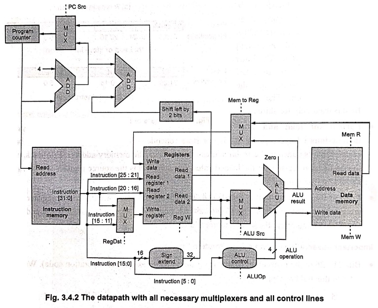
From the above information, we can add the instruction labels and extra
multiplexer (for the Write register number input of the register file) to the
simple datapath. Fig. 3.4.2 shows these additions plus the ALU control block,
the write signals for state elements, the read signal for the data memory and
the control signals for the multiplexers. Since all the multiplexers have two
inputs, they each require a single control line.
•
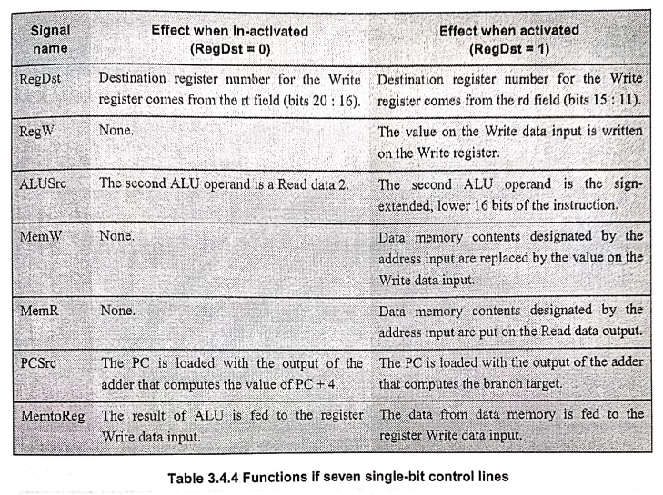
Fig. 3.4.2 shows seven single‒bit control lines (RegDst, RegW, ALUSrc, MemW,
MemR, PCSrc and MemtoReg) plus the 2‒bits ALUOP control signal.
•
Table 3.4.4 describes the function of single‒bit control lines.
•
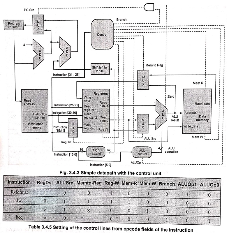
These nine control signals (seven single‒bit control lines and the 2‒bits ALUOp
control signals) can be set according six input signals to the control unit,
which are the opcode bits 31 to 26. Fig. 3.4.3 shows the datapath with the
control unit and the control signals.
•
As shown in Fig. 3.4.3, the input to the control unit is the 6‒bits opcode
field from the instruction.
•
The outputs of the control unit consist of three 1‒bit signals that are used to
control multiplexors (RegDst, ALUSrc and MemtoReg), three signals for controlling
reads and writes in the register file and data memory (RegWrite, MemRead and
MemWrite), a 1‒bit signal used in determining whether to possibly branch
(Branch) and a 2‒bits control signal for the ALU (ALUOP).
•
An AND gate is used to combine the branch control signal and the Zero output
from the ALU; the AND gate output controls the selection of the next PC.
•
Table 3.4.5 defines whether each control signal should be 0, 1 or don't care
(X) for each of the opcode values.
•
For all R‒format instructions (add, sub, AND, OR and slt) the source register
fields are rs and rt, and the destination register field is rd; this defines
how the signals ALUSrc and RegDst are set (See first row of Table 3.4.5).
•
R‒type instruction also writes a register (Reg W = 1), but neither reads nor
writes data memory.
•
For all R‒format instructions, the PC should be unconditionally replaced with
PC + 4. Thus the Branch control signal is 0; otherwise, the PC is replaced by
the branch target if the Zero output of the ALU is also high.
•
The ALUOp field for R‒type instructions is set to 10 to indicate that the ALU
control should be generated from the funct field.
•
The second and third rows of Table 3.4.5 give the control signal settings for
lw and sw. These ALU Src and ALUOp fields are set to perform the address
calculation.
•
The MemRead and MemWrite are set to perform the memory access. Finally, RegDst
and Reg W are set for a load to cause the result to be stored into the rt
register.
•
The branch instruction sends the rs and rt registers to the ALU. The ALUOp
field for branch is set for a subtract (ALU control = 01), which is used to
test for equality.
•
It is important to note that the Mem to Reg field is irrelevant when the Reg W
signal is 0: since the register is not being written, the value of the data on
the register data write port is not used. Thus, the entry Mem to Reg in the
last two rows of Table 3.4.5 is replaced with X for don't care. Don't cares can
also be added to RegDst when Reg W is 0.
3. Operation of the Datapath
1. Datapath for an R‒type Instruction
•
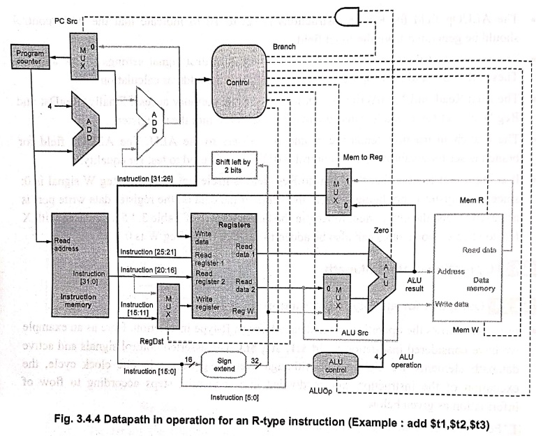
Fig. 3.4.4 shows the operation of the datapath for an R‒type instruction. Here
as an example we have considered instruction: add $t1, $t2, $t3. The asserted control signals and active datapath
elements are highlighted. Although everything occurs in one clock cycle, the
execution of the instruction can be divided into sequential steps according to
flow of information as given below:
1.
Fetch the instruction and increment the PC.
2.
Read data from two registers, $t2 and $t3 and compute the setting of the
control lines using main control unit.
3.
Generate the ALU function using the function code for addition operation (bits
5: 0, which is the function field of the instruction) and perform addition on
the data read from the register file.
4.
Write the result from the ALU into the register file using bits 15: 11 of the
instruction that select the destination register ($t1).
Note: The control lines
datapath units and connections that are active are highlighted.
2. Datapath for Load Word Instruction
•
Fig. 3.4.5 shows the operation of the datapath for load word instruction. Here
as an example we have considered instruction: Iw $t1, offset($t2). The execution of the load instruction can be
divided into sequential steps according to flow of information as given below:
1.
Fetch the instruction and increment the PC.
2.
Read data from register $t2 of register file.
3.
Compute the sum of the value read from the register file and the sign‒extended,
lower 16 bits of the instruction (offset) using ALU.
4.
Use the sum from the ALU as the address for the data memory.
5.
Write the data from the memory unit into the register file; the register
destination is given by bits 20: 16 of the instruction ($t1).
Note: The control lines,
datapath units, and connections that are active are highlighted.
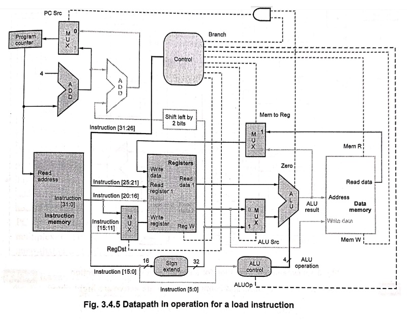
• A load and store instructions operate very similarly. The main differences are that the memory control indicate a write rather than a read, the value of the second register is used for the data to store and the operation of writing the data memory value to the register file is not necessary.
3. Datapath for Branch ‒ On ‒ Equal Instruction
•
Fig. 3.4.6 shows the operation of the datapath for branch‒on‒equal instruction.
Here as an example we have considered instruction: beq $t1, $t2, offset. It operates much like an R‒format
instruction, but the ALU output is used to determine whether the PC is written
with PC + 4 or the branch target address. The execution of the branch‒on‒equal
instruction can be divided into sequential steps according to flow of
information as given below:
1.
Fetch the instruction and increment the PC.
2.
Read data from two registers, $t2 and $t3.
3.
Generate the ALU function using the function code for subtract operation (bits
5: 0, which is the funct field, of the instruction) and perform subtraction on
the data read from the register file. Add the value of PC + 4 to the sign‒extended,
lower 16 bits of the instruction (offset) shifted left by two to get the branch
target address.
4.
Use the Zero result from the ALU to decide which adder result to store into the
PC.
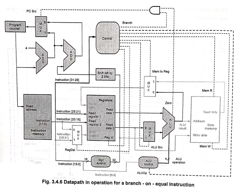
Note: The control
lines, datapath units and connections that are active are highlighted.
4. Finalizing Control
•
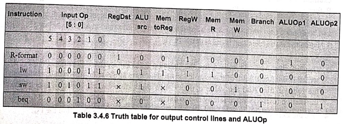
The control function can be precisely defined using the contents of Table
3.4.6. The outputs are the control lines and the input is the 6‒bits opcode
field, Op [5: 0], i.e. bits 31: 26 of the instruction. Thus, we can create a
truth table for each of the outputs based on the binary encoding of the opcodes
as shown in Table 3.4.6.
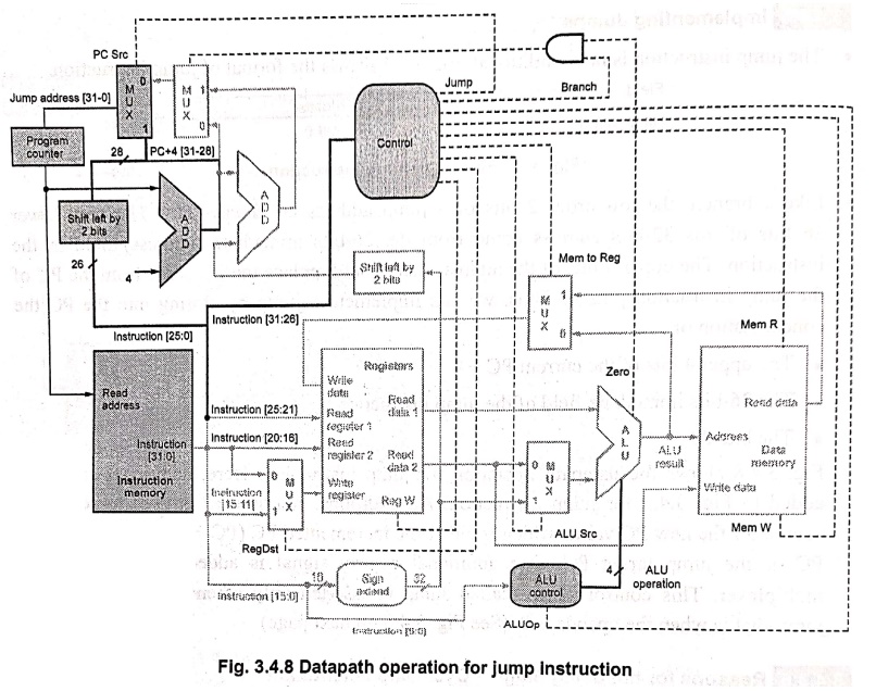
5. Implementing Jumps
•
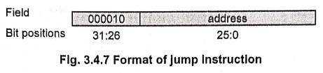
The jump instruction is not conditional. Fig 3.4.7 shows the format of jump
instruction.
•
Like a branch, the low‒order 2 bits of a jump address are always 002.
The next lower 26 bits of this 32‒bits address come from the 26‒bits immediate
(address) field in the instruction. The upper 4 bits of the address that should
replace the PC come from the PC of the jump instruction plus 4. Thus, we can
implement a jump by storing into the PC the concatenation of
■
The upper 4 bits of the current PC + 4
■
The 26‒bits immediate field of the jump instruction
■
The bits 00two
•
Fig. 3.4.8 shows the datapath operation for jump instruction. Here, additional
control is added to Fig. 3.4.3 for jump instruction. An additional multiplexer
is used to select the source for the new PC value, which is either the
incremented PC (PC + 4), the branch target PC or the jump target PC. One
additional control signal is added for the additional multiplexer. This control
signal, called Jump is asserted only when the instruction is a jump‒that is
when the opcode is 2.
6. Reasons for not using Single ‒ Cycle Implementation
1.
It is inefficient. Because the longest possible path in the processor
determines the clock cycle. Remember that the clock cycle must have the same
length for every instruction in single‒cycle design.
2.
The overall performance of a single‒cycle implementation is likely to be poor,
since the clock cycle is too long.
3.
The penalty for using the single‒cycle design with a fixed clock cycle is
significant. Single‒cycle designs for floating‒point unit or an instruction set
with more complex instructions do not work well at all.
4.
It do not improve the worst‒case cycle time. Thus it violates the great idea of
making the common case fast.
Review Questions
1. State the
advantages of multiple levels of decoding.
2. Give instruction
formats for R type, load or store and branch instructions.
3. Draw the simple
combine datapath with all necessary multiplexers and control lines.
4. State the functions
of following control lines.
a) PC Src b) ALU Src c)
RegDst d) Mem R
5. Draw and explain
the simple datapath with the control unit and explain the execution of ALU
instructions.
6. With the help of a
neat diagram explain the operation of datapath for R type instruction.
7. With the help of a
neat diagram explain the operation of datapath for load instruction.
8. Give the sequential
steps required for execution of R‒type instruction.
9. Give the sequential
steps required for execution of load instruction.
10. Explain the
operation of datapath for branch instruction.
11. Give the
sequential steps required for execution of branch operation.
12. Draw the format of
jump instruction.
13. Draw and explain
the datapath operation for jump instruction.
14. State the reasons
for not using single cycle implementation.
15. Explain data path
control in detail.
Computer Organization and Architecture: Chapter 3: Processor Design : Tag: Computer : Processor Design - Simple Implementation Scheme and Drawbacks
Computer Organization and Architecture: Chapter 3: Processor Design
Under Subject
Computer Organization and Architecture
CW25201 3rd Semester IT department. | 2025 Regulation | 3rd Semester 2025 Regulation
Related Subjects
Discrete Mathematics
MA25C14 3rd Semester CSE,IT,CY,AIDS departments. | 2025 Regulation | 3rd Semester 2025 Regulation
Data Structures
CS25C08 3rd Semester CSE,IT,CY,AIDS departments. | 2025 Regulation | 3rd Semester 2025 Regulation
Computer Organization and Architecture
CW25201 3rd Semester IT department. | 2025 Regulation | 3rd Semester 2025 Regulation
Object Oriented Programming
CS25C07 3rd Semester IT department. | 2025 Regulation | 3rd Semester 2025 Regulation
Web Technologies
IT25301 3rd Semester IT department. | 2025 Regulation | 3rd Semester 2025 Regulation
English Communication Skills Laboratory I
EN25C03 3rd Semester all department. | 2025 Regulation | 3rd Semester 2025 Regulation
Skill Development Course I
3rd Semester all department. | 2025 Regulation | 3rd Semester 2025 Regulation