Computer Organization and Architecture: Chapter 3: Processor Design
Pipelined Datapath and Control
Processor Design
Questions: 1. Draw and explain the implementation of two stage instruction pipelining. 2. Draw and explain the implementation of four stage instruction pipelining. 3. Explain implementation of MIPS instruction pipeline. 4. Draw and explain the single cycle datapath with added control to the pipeline datapath. 5. Disscuss about pipelined data path and control. 6. Write down the five stages of instruction executions.
Pipelined
Datapath and Control
•
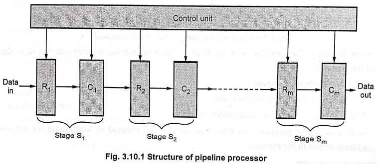
Fig. 3.10.1 shows the general structure of multistage pipeline. As shown in
Fig. 3.10.1, the usually pipeline processor consists of a sequence of m data
processing circuits, called elements,
stages or segments.
•
These stages collectively perform a single operation on a stream of data
operands passing through them. The processing is done part by part in each
stage, but the final result is obtained only after an operand set has passed
through the entire pipeline.
•
Each stage consists of two major blocks: Multiword
input register and datapath circuit.
•
The multiword input registers Ri, hold partially processed results
as they move through the pipeline and they also serves as buffers that prevent
neighbouring stages from interfering with one another. In each clock period the
individual stages process its data and transfers its results to the next stage.
•
The m‒stage pipeline processor shown in Fig. 3.10.1 can simultaneously process
upto m independent sets of data operands. Thus when the pipeline is full, m
separate operations are being executed concurrently, each in a different stage.
This gives a new final result from the pipeline every clock cycle.
•
If time required to perform single suboperation in the pipeline is T seconds
then for m stage pipeline the time required to complete a single operation is
mT seconds. This is called delay or latency of the pipeline.
•
The maximum number of operations completed per second can be given as 1/T. This
is called throughput of the pipeline.
1. Implementation of Two Stage Instruction Pipelining
•
The simplest instruction pipelining breaks instruction processing into two parts:
A fetch stage S1 and an execute
stage S2. When these two stages are overlapped, we get two stage
pipelining with increased throughput.
•
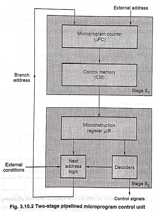
Fig. 3.10.2 shows an implementation of a two‒stage instruction pipeline. The
fetch stage S1 consists of the microprogram counter µPC, which is
the source for microinstruction addresses, and the control memory CM, which
stores the microinstructions.
•
The execution stage S2 consists of microinstruction register μIR,
the decoders that extract control signals from the microinstructions in μIR and
the logic for determining next address or the branch address.
•
The microinstruction register acts as a buffer register for stage S2.
With these two stages it is possible that, while instruction Ii with
address Ai is being executed by stage S2, the instruction
Ii+ 1 with the next consecutive address Ai+1 is fetched
from memory by stage S1. If on executing Ii in S2
it is determined that a branch must be made to a nonconsecutive address, then
the prefetched instruction Ii+ 1 in S1 has to be
discarded. In such cases branch address is obtained directly from μI itself and
fed back to S1. The branch address is then loaded into μPC and next
instruction is fetched from the branch address.
2. Organization of CPU with Four Stage Instruction Pipelining
•
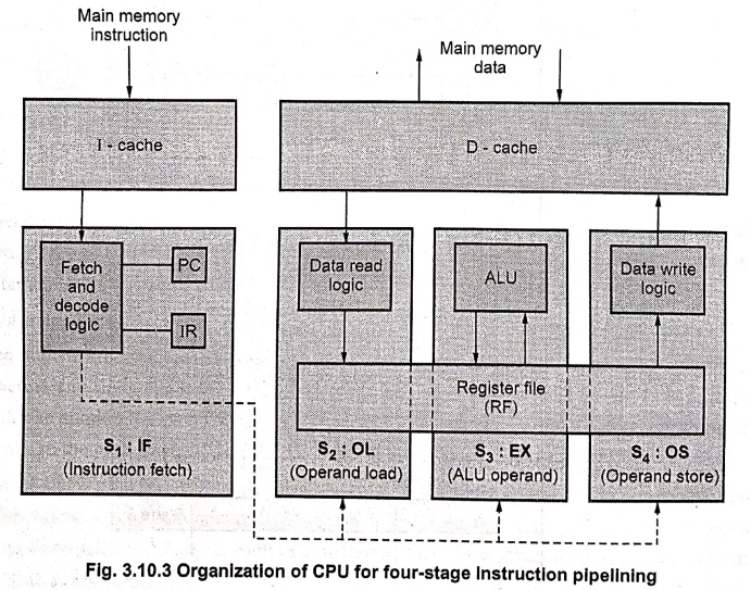
Fig. 3.10.3 shows the implementation of four‒stage instruction pipelining. As
shown in Fig. 3.10.3 the CPU is directly connected to a cache memory, which is
split into instruction and data parts, called the I‒cache and D‒cache,
respectively. This splitting of the cache permits both an instruction word and
a memory data word to be accessed in the same clock cycle.
•
The four stages: Shown in Fig. 3.10.3 perform the following functions:
■
S1 : IF : Instruction
fetching and decoding using the I cache.
■
S2 : OL : Operand loading
from the D‒cache to register file.
■
S3 : EX : Data processing
using the ALU and register file.
■
S4 : OS : Operand storing
to the D‒cache from register file.
•
Stages S2 and S4 implements memory load and store
operations, respectively.
•
Stages S2, S3 and S4 share the CPU's local
Register File (RF). The registers in the register file act as interstage buffer
registers.
•
The stage 3 implements data transfer and data processing operations of the
register to register type using ALU of the CPU.
3. Implementation of MIPS Instruction Pipeline
Fig.
3.10.4 shows the single‒cycle datapath with the pipeline stages. The
instruction execution is divided into five stages means a five‒stage pipeline.
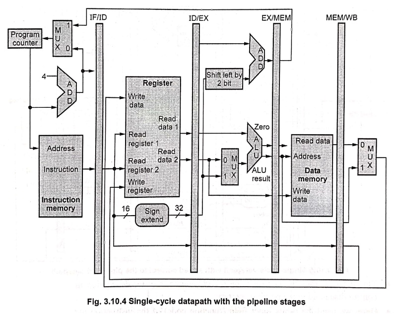
1. IF :
Instruction fetch.
2. ID : Instruction
decode and register file read.
3. EX :
Execution or address calculation.
4. MEM :
Data memory access.
5. WB :
Write back.
•
In this pipeline stages, all instructions advance during each clock cycle from
one pipeline register to the next. The registers are named for the two stages
separated by that register. For example, the pipeline register between the IF
and ID stages is called IF/ID.
4. Pipeline Control
•
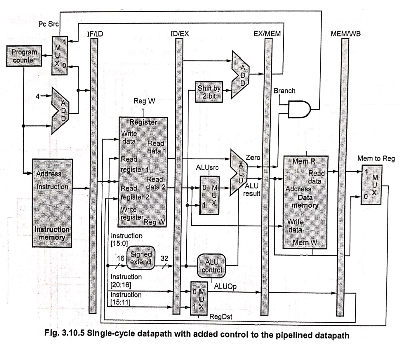
Fig. 3.10.5 shows the single‒cycle datapath with added control to the pipelined
datapath.
•
This datapath uses the control logic for PC source, register destination number
and ALU control discussed in the previous section.
•
Here, we need the 6‒bits funct field (function code) of the instruction in the
EX stage as input to ALU control, so these bits must also be included in the
ID/EX pipeline register.
•
The 6‒bits of funct field are also the 6 least significant bits of the immediate
field in the instruction, so the ID/EX pipeline register can supply them from
the immediate field since sign extension leaves these bits unchanged.
•
We have already assumed that the PC is written on each clock cycle, so there is
no separate write signal for the PC. Similarly, there are no separate write
signals for the pipeline registers (IF/ID, ID/EX, EX/MEM, and MEM/WB), since
the pipeline registers are also written during each clock cycle.
•
As shown in Fig. 3.10.5, each control line is associated with a component
active in only a single pipeline stage. Thus, we can divide the control lines
into five groups according to the pipeline stage.
1. Instruction fetch :
The control signals to read instruction memory and to write the PC are always
asserted, so there is nothing special to control in this pipeline stage.
2. Instruction
decode/register file read : Nothing special to
control in this pipeline stage.
3. Execution/address
calculation : The
signals need to be control are RegDst, ALUOP and ALUSrc. The signals select the
Result register, the ALU operation and either Read data 2 or a sign‒extended
immediate for the ALU.
4. Memory access :
The signals set in this stage are Branch, MemRead and MemWrite. The branch
equal, load, and store instructions set these signals, respectively. The PC Src
selects the next sequential address unless control asserts Branch and the ALU
result equal to 0.
5. Write‒back :
The two control signals set in this stage are Mem to Reg and RegWrite. The Mem
to Reg signal decides between sending the ALU result or the memory value to the
register file, and RegWrite signal writes the chosen value.
•
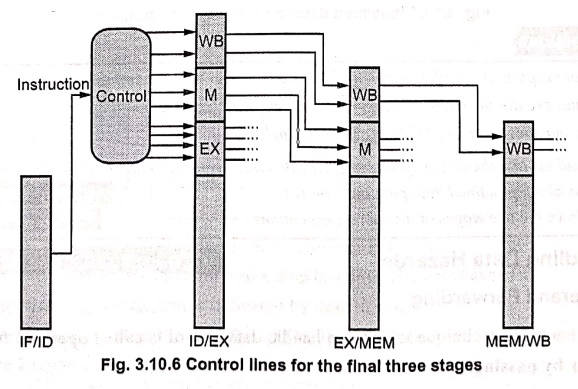
The nine control lines we have seen in Fig. 3.10.6 are grouped here by pipeline
stage. Thus implementing control means setting the nine control lines in each
stage for each instruction.
•
The simplest way to do this is to extend the pipeline registers to include
control information as shown in Fig. 3.10.6.
•
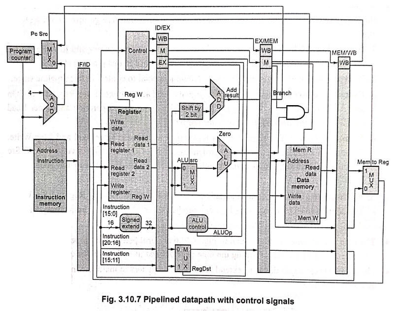
Fig. 3.10.7 shows the full datapath with the extended pipeline registers and
with the control lines connected to the control portions of the pipeline
régisters. The control values for the last three stages are created during the
instruction decode stage and then placed in the ID/EX pipeline register. The
control lines for each pipe stage are used, and remaining control lines are
then passed to the next pipeline stage.
Review Questions
1. Draw and explain
the implementation of two stage instruction pipelining.
2. Draw and explain
the implementation of four stage instruction pipelining.
3. Explain
implementation of MIPS instruction pipeline.
4. Draw and explain
the single cycle datapath with added control to the pipeline datapath.
5. Disscuss about
pipelined data path and control.
6. Write down the five
stages of instruction executions.
Computer Organization and Architecture: Chapter 3: Processor Design : Tag: Computer : Processor Design - Pipelined Datapath and Control
Computer Organization and Architecture: Chapter 3: Processor Design
Under Subject
Computer Organization and Architecture
CW25201 3rd Semester IT department. | 2025 Regulation | 3rd Semester 2025 Regulation
Related Subjects
Discrete Mathematics
MA25C14 3rd Semester CSE,IT,CY,AIDS departments. | 2025 Regulation | 3rd Semester 2025 Regulation
Data Structures
CS25C08 3rd Semester CSE,IT,CY,AIDS departments. | 2025 Regulation | 3rd Semester 2025 Regulation
Computer Organization and Architecture
CW25201 3rd Semester IT department. | 2025 Regulation | 3rd Semester 2025 Regulation
Object Oriented Programming
CS25C07 3rd Semester IT department. | 2025 Regulation | 3rd Semester 2025 Regulation
Web Technologies
IT25301 3rd Semester IT department. | 2025 Regulation | 3rd Semester 2025 Regulation
English Communication Skills Laboratory I
EN25C03 3rd Semester all department. | 2025 Regulation | 3rd Semester 2025 Regulation
Skill Development Course I
3rd Semester all department. | 2025 Regulation | 3rd Semester 2025 Regulation