Computer Organization and Architecture: Chapter 3: Processor Design
Design Conventions of a Processor
Processor Design
Processor Design: Design Conventions of a Processor: 1. Logic Elements 2. Clocking Methodology
Design
Conventions of a Processor
1. Logic Elements
•
The datapath elements in the MIPS implementation consist of two different types
of logic elements: Combinational elements and State elements.
• Combinational
elements ‒ Act on data values
■
Output depends only on current inputs
■
Produces same output for the same input
■
Does not have internal storage
■
Examples: AND gate, multiplexer and ALU
• State
element ‒ Contain internal storage
■
Has at least two inputs:
a.
clock
b.
datain
■
Has at least one output:
dataout
■
Clock determines the writing time instance for state element; reading can occur
anytime from the state element.
■
Output value is same as the value written in earlier clock cycle
■
Output depends on current as well as previous inputs and hence state element is
also called sequential element.
■
Example: Instruction and data memories and registers
2. Clocking Methodology
A
clocking methodology specifies read and write timings for signal. It is
important to specify these timings, because if a signal is written at the same
time it is read, the value of the read may correspond to the old value and
hence may get wrong value. Computer designs cannot tolerate such
unpredictability. A clocking methodology is designed to ensure predictability.
Edge‒triggered clocking
methodology: An edge‒triggered clocking methodology
means that any values stored in a sequential logic element are updated only on
a clock edge. In this methodology, the inputs are values that were written in a
previous clock cycle, while the outputs are values that can be used in a
following clock cycle.
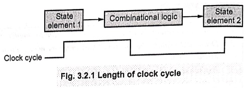
• Length of the clock cycle:
Fig.
3.2.1 shows the two state elements with a block of combinational logic. As shown
in Fig. 3.2.1, signals propagate from state element 1, through the
combinational logic and to state element 2 in the time of one clock cycle. The
time necessary for the signals to reach state element 2 from state element 1
defines the length of the clock cycle.
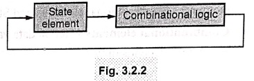
An
edge‒triggered methodology allows a state element to be read and written in the
same clock cycle without creating a race that could lead to indeterminate data
values. As shown in Fig. 3.2.2, it is possible to read the contents of a
register, send the value through some combinational logic and write that
register in the same clock cycle if the clock cycle is long enough so that the
input values are stable when the active clock edge occurs. With an edge‒c
triggered timing methodology, there is no feedback within a single clock cycle
and hence this works correctly.
Computer Organization and Architecture: Chapter 3: Processor Design : Tag: Computer : Processor Design - Design Conventions of a Processor
Computer Organization and Architecture: Chapter 3: Processor Design
Under Subject
Computer Organization and Architecture
CW25201 3rd Semester IT department. | 2025 Regulation | 3rd Semester 2025 Regulation
Related Subjects
Discrete Mathematics
MA25C14 3rd Semester CSE,IT,CY,AIDS departments. | 2025 Regulation | 3rd Semester 2025 Regulation
Data Structures
CS25C08 3rd Semester CSE,IT,CY,AIDS departments. | 2025 Regulation | 3rd Semester 2025 Regulation
Computer Organization and Architecture
CW25201 3rd Semester IT department. | 2025 Regulation | 3rd Semester 2025 Regulation
Object Oriented Programming
CS25C07 3rd Semester IT department. | 2025 Regulation | 3rd Semester 2025 Regulation
Web Technologies
IT25301 3rd Semester IT department. | 2025 Regulation | 3rd Semester 2025 Regulation
English Communication Skills Laboratory I
EN25C03 3rd Semester all department. | 2025 Regulation | 3rd Semester 2025 Regulation
Skill Development Course I
3rd Semester all department. | 2025 Regulation | 3rd Semester 2025 Regulation