Computer Organization and Architecture: Chapter 3: Processor Design
Building a Datapath
Processor Design
Questions: 1. Draw and explain the datapath to implement instruction fetch and PC increment operations. 2. Draw and explain the datapath segment for arithmetic‒logic instructions. 3. Draw and explain the datapath segment for load word and store word instructions. 4. Draw and explain the datapath segment for computation of branch target address. 5. Explain the structure of the datapath segment that handles branches with the help of block diagram. 6. Draw and explain the simple combine datapath for the MIPS architecture. 7. Explain data path in detail. 8. What are R‒Type instructions?
Building a Datapath
• The
MIPS implementation includes, the datapath elements (a unit used to operate on
or hold data within a processor) such as the instruction and data memories, the
register file, the ALU and adders.
• Fig.
3.3.1 shows the combination of the three elements (instruction memory, program
counter and adder) to form a datapath that fetches instructions and increments
the PC to obtain the address of the next sequential instruction.
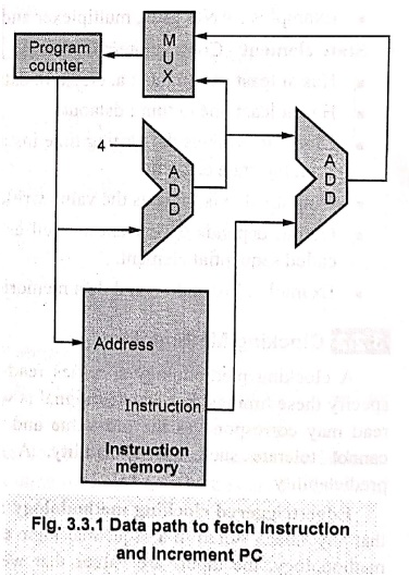
• The instruction memory stores the instructions of a program and gives instruction as an output corresponding to the address specified by the program counter. The adder is used to increment the PC by 4 to the address of the next instruction.
• Since
the instruction memory only reads, the output at any time reflects the contents
of the location specified by the address input and no read control signal is
needed.
•
The program counter is a 32‒bits register that is written at the end of every
clock cycle and thus does not need a write control signal.
•
The adder always adds its two 32‒bits inputs and place the sum on its output.
1. Datapath Segment for Arithmetic ‒ Logic Instructions
• The
arithmetic‒logic instructions read operands from two registers, perform an ALU
operation on the contents of the registers and write the result to a register.
We call these instructions as R‒type
instructions. This instruction class includes add, sub, AND, OR, and slt.
For example, OR $t1, $t2, $t3 reads $t2 and $t3, performs logical OR operation
and saves the result in $t1.
•
The processor's 32 general‒purpose registers are stored in a structure called a
register file. A register file is a
collection of registers in which any register can be read or written by
specifying the number of the register in the file. The register file contains
the register state of the computer.
•
Fig. 3.3.2 shows multiport register file (two read ports and one write port)
and the ALU section of Fig. 3.3.2. We know that, the R‒format instructions have
three register operands: Two source operands and one destination operand.
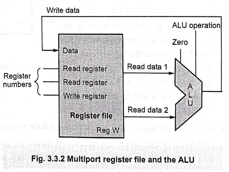
• For each data word to be read from the register file, we need to specify the register number to the register file. On the other hand, to write a data word, we need two inputs: One to specify the register number to be written and one to supply the data to be written into the register.
• The
register file always outputs the contents of whatever register numbers are on
the Read register inputs. Write operations, however, are controlled by the
write control (Reg W) signal. This signal is asserted for a write operation at
the clock edge.
•
Since writes to the register file are edge‒triggered, it is possible to perform
read and write operation for the same register within a clock cycle: The read
operation gives the value written in an earlier clock cycle, while the value
written will be available to a read in a subsequent clock cycle.
• As
shown in Fig. 3.3.2, the register number inputs are 5 bits wide to specify one
of 32 registers, whereas the data input and two data output buses are each 32
bits wide.
2. Datapath Segment for Load Word and Store Word Instructions
•
Now, consider the MIPS load word and store word instructions, which have the
general form lw $t1, offset_value($t2)
or sw $t1, offset_value ($t2).
•
In these instructions $tl is a data register and $t2 is a base register.
The memory address is computed by adding the base register ($t2), to the 16‒bits
signed offset value specified in the instruction.
• In
case of store instruction, the value from the data register ($t1) must be read
and in case of load instruction, the value read from memory must be written
into the data register ($t1). Thus, we will need both the register the file and
the ALU from Fig. 3.3.2.
• We
know that, the offset value is 16‒ bits and base register contents are 32‒ bits.
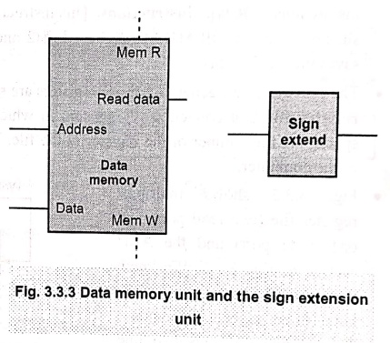
Thus, we need a sign‒extend unit to
convert the 16‒bits offset field in the instruction to a 32‒bits signed value
so that it can be added to base register.
• In
addition to sign extend unit, we need a data
memory unit to read from or write to. The data memory has read and write
control signals to control the read and write operations. It also has an
address input and an input for the data to be written into memory. Fig. 3.3.3
shows these two elements.
• Sign
extension is implemented by replicating the high‒order sign bit of the original
data item in the high‒order bits of the larger, destination data item.
• Therefore,
two units needed to implement loads and stores, in addition to the register
file and ALU of Fig. 3.3.2, are the data memory unit and the sign extension
unit.
3. Datapath Segment for Branch Instruction
•
The beq instruction has three
operands, two registers that are compared for equality and a 16‒bits offset
which is used to compute the branch target address relative to the branch
instruction address. It has a general form: beq $t1, $t2, offset.
•
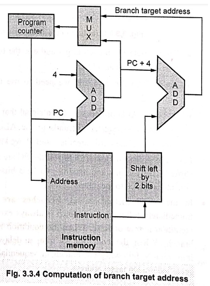
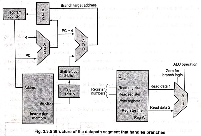
To implement this instruction, it is necessary to compute the branch target
address by adding the sign‒extended offset field of the instruction to the PC.
The two important things in the definition of branch instructions which need
careful attention are:
■
The instruction set architecture specifies that the base for the branch address
calculation is the address of the instruction following the branch (i.e., PC +
4 the address of the next instruction.
■
The architecture also states that the offset field is shifted left 2 bits so
that it is a word offset; this shift increases the effective range of the
offset field by a factor of 4.
•
Therefore, the branch target address is given by
Branch
target address = PC+4+ offset (shifted left 2 bits)
•
In addition to computing the branch target address, we must also see whether
the two operands are equal or not. If two operands are not equal the next
instruction is the instruction that follows sequentially (PC PC + 4); in this
case, we say that the branch is not
taken. On the other hand, if two operands are equal (i.e., condition is
true), the branch target address becomes the new PC, and we say that the branch is taken.
•
Thus, the branch datapath must perform two operations: Compute the branch
target address and compare the register contents.
•
Fig. 3.3.5 shows the structure of the datapath segment that handles branches.
■
To compute the branch target address, the branch datapath includes a sign
extension unit, shifter and an adder.
■
To perform the compare, we need to use the register file and the ALU shown in
Fig. 3.3.2.
■
Since the ALU provides an Zero
signal that indicates whether the result is 0, we can send the two register
operands to the ALU with the control set to do a subtract operation. If the
Zero signal is asserted, we know that the two values are equal.
•
For jump instruction lower 28 bits of the PC are replaced by lower 26 bits of
the instruction shifted left by 2 bits and making two LSB bits = 0. This can be
implemented by simply concatenating 00 to the jump.
•
In the MIPS instruction set, branches
are delayed, meaning that the instruction immediately following the branch
is always executed, independent of whether the branch condition is true or
false. When the condition is false, the execution looks like a normal branch.
When the condition is true, a delayed branch first executes the instruction
immediately following the branch in sequential instruction order before jumping
to the specified branch target address.
4. Creating a Single Datapath
•
We can combine the datapath components needed for the individual instruction
classes into a single datapath and add the control to complete the
implementation.
•
This simplest datapath will attempt to execute all instructions in one clock
cycle. This means that no datapath resource can be used more than once per
instruction, so any element needed more than once must be duplicated. We
therefore need a memory for instructions separate from one for data. We need
the functional units to be duplicated and many of the elements can be shared by
different instruction flows.
•
To share a datapath element between two different instruction classes, we have
connected multiple connections to the input of an element and used a
multiplexer and control signal to select among the multiple inputs.
Example: 1
Show how to build a
datapath for the operational portion of the memory‒ reference and arithmetic‒logical
instructions that uses a single register file and a single ALU to handle both
types of instructions, adding any necessary multiplexers.
Solution:
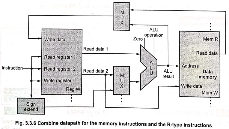
To
create a datapath with only a single register file and a single ALU, we must
support two different sources for the second ALU input, as well as two
different sources for the data stored into the register file. Thus, one
multiplexer is placed at the ALU input and another at the data input to the
register file. Fig. 3.3.6 shows the operational portion of the combined
datapath.
•
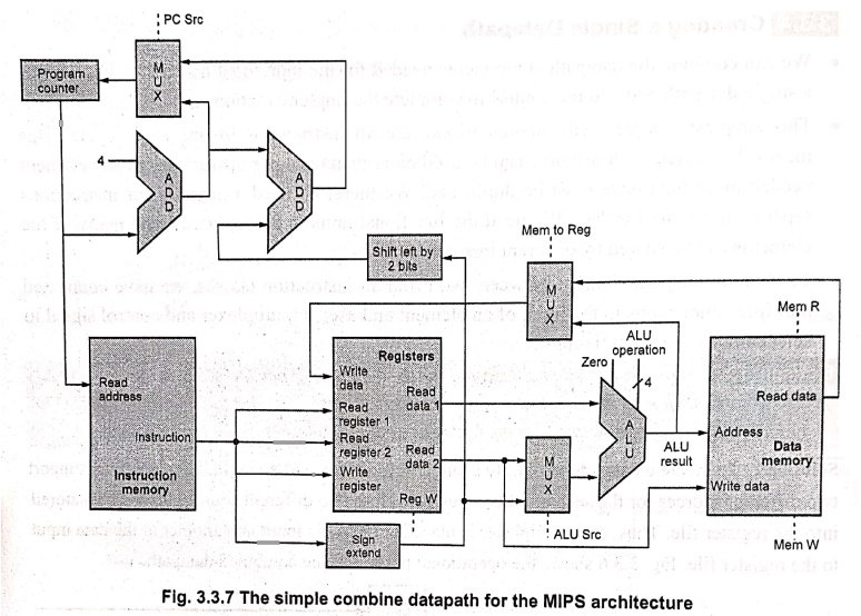
We can make a simple datapath for the core MIPS architecture by adding the
datapath for instruction fetch, the datapath from R‒type and memory
instructions, and the datapath for branches as shown in Fig. 3.3.7.
Review Questions
1. Draw and explain
the datapath to implement instruction fetch and PC increment operations.
2. Draw and explain
the datapath segment for arithmetic‒logic instructions.
3. Draw and explain
the datapath segment for load word and store word instructions.
4. Draw and explain
the datapath segment for computation of branch target address.
5. Explain the
structure of the datapath segment that handles branches with the help of block
diagram.
6. Draw and explain
the simple combine datapath for the MIPS architecture.
7. Explain data path
in detail.
8. What are R‒Type
instructions?
Computer Organization and Architecture: Chapter 3: Processor Design : Tag: Computer : Processor Design - Building a Datapath
Computer Organization and Architecture: Chapter 3: Processor Design
Under Subject
Computer Organization and Architecture
CW25201 3rd Semester IT department. | 2025 Regulation | 3rd Semester 2025 Regulation
Related Subjects
Discrete Mathematics
MA25C14 3rd Semester CSE,IT,CY,AIDS departments. | 2025 Regulation | 3rd Semester 2025 Regulation
Data Structures
CS25C08 3rd Semester CSE,IT,CY,AIDS departments. | 2025 Regulation | 3rd Semester 2025 Regulation
Computer Organization and Architecture
CW25201 3rd Semester IT department. | 2025 Regulation | 3rd Semester 2025 Regulation
Object Oriented Programming
CS25C07 3rd Semester IT department. | 2025 Regulation | 3rd Semester 2025 Regulation
Web Technologies
IT25301 3rd Semester IT department. | 2025 Regulation | 3rd Semester 2025 Regulation
English Communication Skills Laboratory I
EN25C03 3rd Semester all department. | 2025 Regulation | 3rd Semester 2025 Regulation
Skill Development Course I
3rd Semester all department. | 2025 Regulation | 3rd Semester 2025 Regulation