Electron Devices: Chapter 1: Semiconductor
Conductivity of Extrinsic Semiconductor
Questions: 1. Obtain the expressions for conductivity of n‒type and p‒type materials. 2. Solved Example Problems
Conductivity
of Extrinsic Semiconductor
•
In an extrinsic semiconductors, there are two types of materials n‒type and p‒type.
1. Conductivity of n‒Type Material
•
It is known that in n‒type material, the free electrons are majority carriers
while the holes are minority carriers.
Let
nn = Concentration of free electrons in n type
Pn
= Concentration of holes in n type
ND
= Concentration of donor atoms
Key
Point: In the symbol, main letter n or p indicates
concentration of type of charge carrier electron or hole while the suffix
indicates the type of material i.e. n‒type or p‒type. Thus nn
indicates electron concentration in n‒type material while np
indicates electron concentration in p‒type material and so on.
•
From the basic equation of conductivity, the conductivity of n‒type material
can be expressed as,
σn = (nnμn + Pnμp)q
•
But Pn<<nn as holes are in minority hence,
σn ≈ nnμnq
•
The number of free electrons is dominantly controlled by donor atoms added than
the thermal at generation room temperature. Hence concentration of donor atoms
ND added can be approximately assumed to be equal to the
concentration of free electrons nn in n type materials.
•
Thus as ND >> ni we can write,
nn = ND and σn
≈ NDμnq
2. Conductivity of p‒Type Material
•
For a p type material, holes are in majority and electrons are in minority.
Let
nP
= Concentration of free electrons in p type
pP
= Concentration of holes in p type
NA
= Concentration of acceptor atoms
•
Thus the conductivity of p type material can be expressed as,
σp = (npμn + PPμP)
q
•
But np<< PP as free electrons are in minority hence,
σp ≈ Pp μp q
The
number of holes is dominantly controlled by added acceptor impurity than the
thermal generation. Each added impurity atom creats a hole hence NA
>> ni. Thus all the holes generated can be approximately
assumed to be equal to the concentration of acceptor NA. Thus,
Pp = NA
And
σp = NA
μp q
Properties of Silicon and Germanium
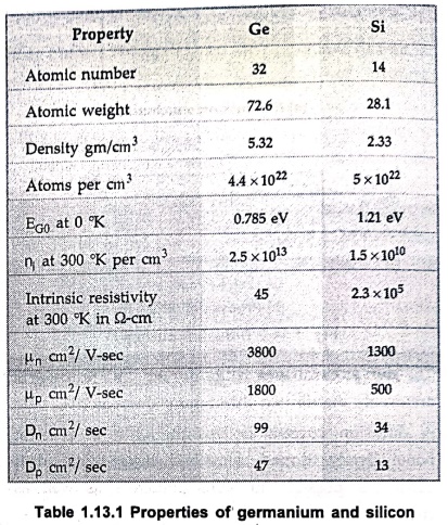
Table 1.13.1 Properties
of germanium and silicon
Ex. 1.13.1 If a donor
impurity is added to the extent of one atom per 108 germanium atoms,
calculate its resistivity at 300 °K. If its resistivity without addition of
impurity at 300 °K is 44.64 Ω‒cm, comparing two values, comment on the result.
Assume: μn =
3800 cm2/V‒sec.
Solution:
Referring
to Table 1.13.1 of properties of germanium, germanium has
4.4× 10²² atoms/cm3.
For
108 germanium atom there is 1 atom impurity added, as given.
Thus,
for 4.4× 10²² germanium atoms, we have,
=
4.4×10²² / 1080
=
4.4× 10¹⁴ atoms of impurity/cm3
This
is nothing but concentration of donor atoms i.e. ND
ND = 4.4 × 10¹⁴ per cm3
= 4.4 × 10¹⁴ / 10‒6
=
4.4× 10²⁰ per m3
Now
as donor impurity is added, n‒type material will form,
σn = nn μn q
= ND μn q
where
nn
= ND
and
μn
= 3800 cm2/V‒sec
=
3800 × 10‒4 m2/V‒sec
σn
= 4.4× 1020 × 3800 × 10‒4 × 1.6 × 10‒19
=
26.752 (Ω‒m)‒1
Resistivity
= ρn = 1/σn
=
1 / 26.752
=
0.0373 Ω‒m = 3.73 Ω ‒ cm
Comment:
Comparing this with resistivity of intrinsic germanium it can be observed that
resistivity reduces considerably due to addition of impurity. Hence
conductivity of n‒type material is much higher and hence it can carry more
current as compared to the intrinsic semiconductor. By controlling amount of
doping we can control the conductivity.
Review
Questions
1. Obtain the expressions for conductivity of n‒type and p‒type
materials.
2. Consider silicon at room temperature of 27 °C. Assuming μn
= 1350 cm3/V‒s and μP=0.048m2/V‒s, find
conductivity if silicon is doped with
a) ND = 5×10¹⁶/cm3,
b) NA=5×10¹⁶/cm3
[Ans.:
10.8 (Ω‒cm)‒1, 3.84 (Ω‒cm)‒1]
Electron Devices: Chapter 1: Semiconductor : Tag: electronics : - Conductivity of Extrinsic Semiconductor
Electron Devices: Chapter 1: Semiconductor
Under Subject

Electron Devices
EC25C01 2nd Semester ECE Dept | 2025 Regulation | 2nd Semester 2025 Regulation
Related Subjects

English Essentials II
EN25C02 2nd Semester | 2025 Regulation | 2nd Semester 2025 Regulation

Tamils and Technology தமிழர்களும் தொழில்நுட்பமும்
UC25H02 2nd Semester | 2025 Regulation | 2nd Semester 2025 Regulation

Linear Algebra
MA25C02 2nd Semester | 2025 Regulation
Electron Devices
EC25C01 2nd Semester ECE Dept | 2025 Regulation | 2nd Semester 2025 Regulation

Data Structures using CPlusPlus
CS25C05 2nd Semester ECE Dept | 2025 Regulation | 2nd Semester 2025 Regulation

Circuits and Network Analysis
EC25C02 2nd Semester ECE Dept | 2025 Regulation | 2nd Semester 2025 Regulation

Re-Engineering for Innovation
ME25C05 2nd Semester | 2025 Regulation | 2nd Semester 2025 Regulation

Engineering Drawing - Laboratory
ME25C01 2nd Semester | 2025 Regulation | 2nd Semester 2025 Regulation

Data Structures using CPlusPlus - Laboratory
CS25C05 2nd Semester ECE Dept | 2025 Regulation | 2nd Semester 2025 Regulation

Devices and Circuits Laboratory
EC25C03 2nd Semester ECE Dept | 2025 Regulation | 2nd Semester 2025 Regulation