Electron Devices: Chapter 1: Semiconductor
Energy Band Diagram for Extrinsic Semiconductors

When impurities are added, allowable energy levels are introduced.
Energy
Band Diagram for Extrinsic Semiconductors
•
When impurities are added, allowable energy levels are introduced.
•
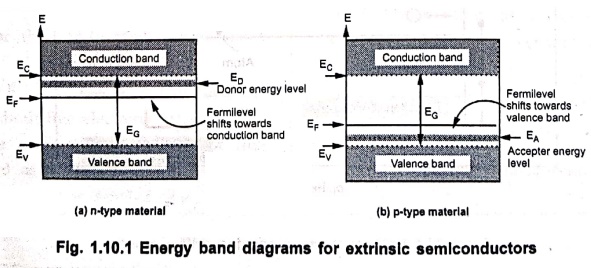
In n‒type material, each donor atom donates one free electron and hence donor
energy level is introduced just below the conduction band denoted as ED.
•
This is so close to the conduction band that even at room temperature, almost
all the added electrons jump into conduction band.
•
Thus probability of occupying energy level by an electron is very high near conduction
band. Hence fermi level EF shifts towards conduction band in n‒type
material.
•
While in p‒type material each acceptor atom creates hole in the valence band.
•
This introduces accpetor energy level very close to valence band but just above
it. It is denoted as EA
•
At room temperature, electrons from valence band jump to acceptor energy level
creating holes in the valence band. This shifts the fermi level EF
towards valence band in p‒type material.
•
The energy band diagrams for n and p‒type materials is shown in Fig. 1.10.1.
Electron Devices: Chapter 1: Semiconductor : Tag: electronics : - Energy Band Diagram for Extrinsic Semiconductors
Electron Devices: Chapter 1: Semiconductor
Under Subject

Electron Devices
EC25C01 2nd Semester ECE Dept | 2025 Regulation | 2nd Semester 2025 Regulation
Related Subjects

English Essentials II
EN25C02 2nd Semester | 2025 Regulation | 2nd Semester 2025 Regulation

Tamils and Technology தமிழர்களும் தொழில்நுட்பமும்
UC25H02 2nd Semester | 2025 Regulation | 2nd Semester 2025 Regulation

Linear Algebra
MA25C02 2nd Semester | 2025 Regulation
Electron Devices
EC25C01 2nd Semester ECE Dept | 2025 Regulation | 2nd Semester 2025 Regulation

Data Structures using CPlusPlus
CS25C05 2nd Semester ECE Dept | 2025 Regulation | 2nd Semester 2025 Regulation

Circuits and Network Analysis
EC25C02 2nd Semester ECE Dept | 2025 Regulation | 2nd Semester 2025 Regulation

Re-Engineering for Innovation
ME25C05 2nd Semester | 2025 Regulation | 2nd Semester 2025 Regulation

Engineering Drawing - Laboratory
ME25C01 2nd Semester | 2025 Regulation | 2nd Semester 2025 Regulation

Data Structures using CPlusPlus - Laboratory
CS25C05 2nd Semester ECE Dept | 2025 Regulation | 2nd Semester 2025 Regulation

Devices and Circuits Laboratory
EC25C03 2nd Semester ECE Dept | 2025 Regulation | 2nd Semester 2025 Regulation