Electron Devices: Chapter 1: Semiconductor
Semiconductor: Important Example Solved Problems
Electron Devices
Electron Devices: Chapter 1: Semiconductor : Anna University Solved Problems, Assignment Problems and Important Solved Problems
Electron
Devices
Chapter
1: Semiconductor
Important
Example Solved Problems
Mobility of Charged Particle
Ex.1 A bar of intrinsic
germanium 6 cm long is subjected to a potential difference of 12 V. If the
velocity of electrons in bar is 73 m/s, determine the mobility of electrons.
Solution: The given values are,
1 = 6 cm = 6×10‒2 m,
V = 12 V,
v
= 73 m/sec
E=Electric
field intensity
=
V / l = 12 / [6×10‒2] = 200 V/m
Now
v = μ E
73
= μ. × 200
Μ
= Mobility = 73/200
=
0.3650 m2/V-sec
=
3650 cm2/V-sec
General Expression for Conductivity (σ)
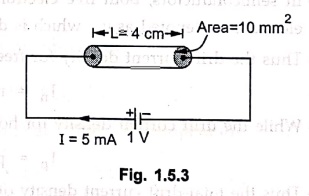
Ex. 2: A bar of n type silicon has
length of 4 cm and circular cross‒section of 10 mm2. When it is
subjected to a voltage of 1 V applied across its length, the current flowing
through it is 5 mA. Calculate i) Concentration of free electrons. ii) Drift
velocity of electrons.
Assume ‒ Charge on one
electron as 1.6 × 10‒19 C.
Mobility of free electron
as 1300 cm2/V‒s.
Solution:
The
bar is shown in Fig. 1.5.3.
Current density J = I/A = 5×10‒3 / 10×10‒6
= 500 A/m2
The
current density is also given by,
J
= nqμE ………..(1)
where
E
= Field intensity = V/L
=
1 / 4×10‒2
= 25 V/m
q
= Charge on electron = 1.6×10‒19 C
μ = Mobility = 1300 cm2/V‒s = 0.13
m2/V‒s
Substituting
all the values in equation (1),
500
= n×1.6×10‒19 × 0.13×25
i.e.
n = 0.9615×10²¹ per m3
Drift
velocity v = μ E = 0.13×25 = 3.25 m/s
... Drift velocity
Intrinsic Concentration and
Conductivity of Intrinsic Semiconductor
Ex. 3: Find the resistivity of an
intrinsic silicon at 300 °K if intrinsic concentration of silicon at 300 °K is
1.5×1010 cm3 per while μn = 1300 cm2/V‒sec
and μp= 500 cm2/V‒sec. Assume q=1.6×10‒19 C.
Solution:
The
given values are, ni = 1.5×10¹⁰/cm3
ni
= 1.5× 10¹⁰ / 10‒6 /m3
= 1.5×10¹⁶/m3
And
μn
= 1300×10‒4 m2/V‒sec,
μр
= 500×10‒4 m2/V‒sec
Now
σi = ni (μn +
μp) q
=
1.5 × 10¹⁶ [1300 + 500] × 10-4 × 1.6×10‒19
= 0.000432 (Ω-m)-1 ………. Conductivity
ρ = 1/σi = 1/0.000432 = 2314.8148 Ω‒m …….Resistivity
The
resistivity is reciprocal of conductivity.
Ex. 4: Calculate the intrinsic
concentration of Germanium in carriers/m3 at a temperature of 320 °K
given that ionization energy is 0.75 eV and Boltzmann's constant k = 1.374× 10‒23
J/°K. Also calculate the intrinsic conductivity given that the motilities of
electrons and holes in pure germanium are 0.36 and 0.17 m2/volt ‒
sec respectively.
Solution:
The
temperature dependence of ni is,
ni = BT3/2 e‒EG0/2kT
B
= Constant, EG0 = Energy gap at absolute zero,
k
= Boltzmann's constant
At
300°K,
ni = 2.5 × 10¹³/cm3
= 2.5 × 10¹⁹/m3
k = 1.374 × 10‒23 J/°K
and
1 eV = 1.374×10‒23 / 1.6×10‒19
eV/°K = 8.58 × 10‒5 eV/°K
2.5 × 1019 = B (300)3/2 e‒0.75/2
× 8.58 × 10‒5 × 300
B
= 1.0218 × 10²²
At
T = 320°K,
n1 = 1.0218 × 1022 ×
(320)3/2 e‒0.75/2 × 8.58 × 10‒5 × 320 = 6.84 ×
1019/m3
σi = ni (μn
+μp) q = 6.84 × 10¹⁹ (0.36 + 0.17) × 1.6 × 10‒19
=
5.8 (Ω-m)‒1
…….
Conductivity at 320°K
Conductivity of Extrinsic Semiconductor
Ex. 5: If a donor impurity is
added to the extent of one atom per 108 germanium atoms, calculate
its resistivity at 300 °K. If its resistivity without addition of impurity at
300 °K is 44.64 Ω‒cm, comparing two values, comment on the result.
Assume: μn =
3800 cm2/V‒sec.
Solution:
Referring
to Table 1.13.1 of properties of germanium, germanium has
4.4× 10²² atoms/cm3.
For
108 germanium atom there is 1 atom impurity added, as given.
Thus,
for 4.4× 10²² germanium atoms, we have,
=
4.4×10²² / 1080
=
4.4× 10¹⁴ atoms of impurity/cm3
This
is nothing but concentration of donor atoms i.e. ND
ND = 4.4 × 10¹⁴ per cm3
= 4.4 × 10¹⁴ / 10‒6
=
4.4× 10²⁰ per m3
Now
as donor impurity is added, n‒type material will form,
σn = nn μn q
= ND μn q
where
nn
= ND
and
μn
= 3800 cm2/V‒sec
=
3800 × 10‒4 m2/V‒sec
σn
= 4.4× 1020 × 3800 × 10‒4 × 1.6 × 10‒19
=
26.752 (Ω‒m)‒1
Resistivity
= ρn = 1/σn
=
1 / 26.752
=
0.0373 Ω‒m = 3.73 Ω ‒ cm
Comment:
Comparing this with resistivity of intrinsic germanium it can be observed that
resistivity reduces considerably due to addition of impurity. Hence
conductivity of n‒type material is much higher and hence it can carry more
current as compared to the intrinsic semiconductor. By controlling amount of
doping we can control the conductivity.
Law of Mass Action
Ex. 6: Calculate the majority and
minority carrier concentrations in silicon at room temperature of 27° C if
a) NA =1017/cm3
and b) ND = 5×10¹⁵/cm3
Solution:
a)
As impurity is acceptor, the material is p‒type.
Pp
= Majority carrier concentration = NA =1017/cm3
For
p‒type,
np×Pp
= ni2
.... Law of mass action
ni
= 1.5 × 10¹⁰ /cm3
…….From Table 1.13.1
np = ni2
/ Pp = 2.25 × 10³ /cm3
Minority carrier concentration
b)
As impurity is donor, the material is n‒type
nn = Majority carrier concentration
= ND = 5 × 10¹⁵ /cm3
For
n‒type,
nn × Pn = ni2
Law of mass action
ni = 1.5 × 10¹⁰ /cm3
Basic material same
Pn = ni2 / nn
= 45 × 103 /cm3
Minority carrier concentration
Ex. 7: A bar of silicon 0.1 cm
long has a cross‒sectional area of 8 × 10‒8 m2, heavily
doped with phosphorous. What will be the majority carrier density resulting
from doping if bar is to have a resistance of 1.5 kΩ?
Given: For silicon at room
temperature, μn = 0.14 m2/ V‒sec, μp = 0.05 m2/V‒sec,
ni = 1.5×10¹⁰ per cm3.
Solution: :
R = ρl /
A
where
l = 0.1 cm = 0.1× 10⁻²
m,
A = 8×10‒8 m2, R = 1.5 kΩ
ρ = RA/l
= [ 1.5×103 × 8×10‒8
] / 0.1× 10‒2
= 0.12 Ω ‒ m
Conductivity.
σ = 1/ ρ = 1/ 0.12 = 8.333 (Ω‒m)‒1
But
σ = σn = (nnμn+PpμP)q
This
is because phosphorous is donor impurity and will form n‒type material.
According
to law of mass action for n‒type material,
nn
Pn = ni2
pn = ni2
/ nn
σn = (nnμn+PpμP)q
σn = (nnμn+(
ni2 / nn)μP)q
σn = (nn2μn+
ni2μP)q
nn × 8.333 = [ nn2
× 0.14 + (1.5 × 10¹⁰ / 10‒6)2 × 0.05 ] 1.602 ×
10‒19
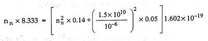
0.14nn2
‒5.201× 10¹⁹ nn + 1.125× 1031 = 0
Solving,
nn = 3.715 × 10²⁰ per m3
(neglecting other value as comparable to ni)
nn = ND
This
is majority carrier density.
Ex. 8: Find the concentration of
holes and electrons in a p type silicon at 300 °K assuming its resistivity in a
p type silicon as 300 °K assuming its resistivity as 0.02 Ω‒cm, μp =
475 cm2 / V ‒ sec, ni = 1.45 ×10¹⁰ per cm3.
Solution:
ρ = Resistivity = 0.02 Ω‒cm = 0.02 × 10‒2
Ω‒m
The
material is p type and its conductivity is,
σP = 1/ρ = 1 / 0.02×10‒2
= 5×10³ (Ω‒m) ‒1
But
σP
= NAμp q
where
q = 1.6 x 10‒19 C,
μp
= 475 cm2/V‒sec = 475 × 10‒4 m2 / V‒sec
5×103
= NA × 475 × 1.6 × 10−19 ×10‒4
NA = 6.5789 × 10²³ per m3
But
Pp = NA = 6.5789 × 10²³
per m3
Concentration
of holes
Using
law of mass action, Pp × np = ni2
And
ni
= 1.45 × 10¹⁰ / 10‒6
per m3
np
= ni2 / Pp = (1.45 × 10¹⁶)2 / 6.5789×1023
=
3.1958 × 10⁸ per m3
Concentration
of electrons
Ex. 9: Find the concentration of
holes and electrons in a p‒type Germanium at 300 °K, if the conductivity is 100
per ohm‒cm. Also find these values for n‒type silicon, if the conductivity is
0.1 per ohm‒cm. Given that
For Germanium ni
= 2.5×10¹³/cm, μn = 3800 cm2/v‒s, μp
= 1800 cm2/v ‒ s
For silicon, ni =
1.5×10¹⁰ per cm3, μn = 1300 cm2/v ‒
s and μp = 500 cm2/v ‒ s
Solution:
Case
1: p‒type Germanium
ni
= 2.5×10¹³/cm3 = 2.5×10¹³ / 10-6 /m3
=
2.5×10¹⁹/m3
μn
= 3800 cm2/V‒s = 3800×10-4 m2/V‒s
μр=
1800 cm2/V‒s = 1800×10‒4 m2/V‒s
σр
= NAμpe where σ =
100 (Ω‒cm)‒1
100
/ 10‒2 = NA×1800×10‒4×1.6×10‒19 i.e. NA = 3.47×10²³/m3
Pp
= NA = 3.47 × 10²³/m3
... Concentration of holes
np
= ni2 / PP = ni2 / NA
=
(2.5×10¹⁹)2 /
3.47×1023
=
1.8×10¹⁵/m3
...
Concentration of electrons
case
2: n‒type Silicon
ni
= 1.5×10¹⁰/cm3 = 1.5×10¹⁰ / 10-6 /m3
=
1.5×10¹⁶/m3
μn
= 1300 cm2/V‒s = 1300×10-4 m2/V‒s
μр=
500 cm2/V‒s = 500×10‒4 m2/V‒s
σn
= NDμnq where σn
= 0.1 (Ω‒cm)‒1
0.1
/ 10‒2 = ND×1300×10‒4×1.6×10‒19 i.e. ND = 4.807×10²⁰/m3
nn
= ND = 4.807 × 10²⁰/m3
... Concentration of electrons
pn
= ni2 / nn = ni2 / ND
=
(1.5×10¹⁶)2 /
4.807×1020
=
4.68×10¹¹/m3
...
Concentration of holes
Equation of Charge Neutrality
Ex. 10: In a sample of germanium at
300 °K, it is found that donor concentration is 2×10¹⁴ atoms/cm3
and acceptor concentration is 3× 10¹⁴ atoms/cm3.
Determine the actual
concentrations of free electrons and holes in the sample. Will it behave as p‒type
or n‒type? Assume ni at 300 °K = 2.5 × 10¹³ per cm3.
Solution:
In
this sample,
ND = 2×10¹⁴ atoms/cm3
= 2×10¹⁴ / 10‒6 = 2×10²⁰ m3
NA = 3×10¹⁴ atoms/cm3
= 3×10¹⁴ / 10‒6 = 3×10²⁰ m3
Using
equation of charge neutrality, p + ND = n + NA.
NA
‒ ND = p‒n
3×10²⁰ ‒ 2×1020 = p‒n
i.e.
p = n + 1×10²⁰
where
p and n are actual concentrations of holes and electrons.
ni = 2.5×10¹³ per cm3
= 2.5×10¹³ / 10‒6
=
2.5×10¹⁹ per cm3
According
to law of mass action, np = ni2
n (n + 1×10²⁰) = (2.5 × 10¹⁹)2
i.e. n2 + 1×10²⁰n
− 6.25×1038 = 0
Solving
n
= 5.901×10¹⁸ electrons/m3
p
= 1.059×10²⁰ holes/m3
As holes are much more than electrons, sample
will behave as p‒type.
Ex. 11: A sample of Ge is doped to
the extent of 1014 donor atoms/cm3 and 7 × 10¹³
acceptor atoms/cm3. At the temperature of the sample, the
resistivity of pure Ge is 60 ohm‒cm. If the applied electric field is 2 V/cm,
find the total conduction current density.
Solution:
ND = 1014/cm3
and NA =7×10¹³/cm3
ρi = 60 Ω‒cm
J = (nμn + Pμp) qE
…….. μn = 3800, μp =
1800
According
to law of electrical neutrality,
ND + P = NA + n
i.e.
n‒p = 3 × 10¹³
According
to law of mass action, np =ni2
σi
= ni(μn+μp) q
i.e.
1/ρi = ni (μn+ μp) q
1/60
= ni (3800 + 1800) × 1.6 × 10‒19
i.e.
n=1.86 × 10¹³/cm3
Solve
equations (1) and (2) to obtain n and p as,
n
= 3.88×10¹³/cm3 and
p=0.88×10¹³/cm3
J = (3.88 × 1013 × 3800 + 0.88 × 1013
× 1800) × 1.6 × 10‒19 × 2 = 0.0522 A/cm
Diffusion Current and Diffusion
Current Density
Ex. 12: Find out the diffusion
constant of holes if their mobility is given as 0.039 m2/v‒sec.
Solution:
μp = 0.039 m2/V‒s
According
to Einstein's relation, Dp / μр = KT
At 300 °K,
Dp
/ μр = Dp / 0.039 = 26 × 10‒3
i.e.
Dp = 1.01 × 10‒3
Ex. 13: The phosphrous (donor)
concentration in a region of a silicon crystal varies linearly from a
concentration of n0 = 1014 cm‒3 at x = 0 mm to
a concentration of n1 = 1017 cm-3 at x = 1 mm.
The diffusion constant for electrons is
Dn = 22.5 cm2/s, the diffusion constant for holes
is Dp = 5.2 cm2/s and the temperature is 300 °K. What is
the diffusion current density in the
positive x‒direction?
Solution:
n0 = 1014 cm-3
n1 = 1017 cm-3,
x1
= 1 mm,
x0
= 0 mm,
Dn = 22.5 × 10⁻⁴ m2/s,
Dp
= 5.2 × 10⁻⁴ m2/s.
For
silicon, ni = 1.5 × 1010 cm‒3
ni2 = np
... Law of mass action
P0 = ni2 / n0
= (1.5×10¹⁰)2 / 1014 = 2.15 × 10⁶
cm-3
P1
= ni2 / n1 = (1.5×10¹⁰)2
/ 1017 = 2.15 × 103 cm-3
dp/dx
= [P1‒P0] / [x1‒x0] = [ 2.25×10³
‒ 2.25×10⁶] / 10‒1 = ‒2.248 × 107 cm‒4
dn/dx = [n1‒n0] / [x1‒x0]
= [1017 ‒ 1014] / 10‒1 = 9.99 × 10¹⁷
cm‒4
J = Jn + Jp = [ qDn
dn/dx ] ‒ [ qDp dp/dx ]
=
1.602×10‒19 [ 22.5×9.99×1017 ‒ 5.2×(‒2.248×10⁷)]
=
3.6 A/cm2
=
3.6×10⁴ A/m2
Electron Devices: Chapter 1: Semiconductor : Tag: electronics : Electron Devices - Semiconductor: Important Example Solved Problems
Electron Devices: Chapter 1: Semiconductor
Under Subject

Electron Devices
EC25C01 2nd Semester ECE Dept | 2025 Regulation | 2nd Semester 2025 Regulation
Related Subjects

English Essentials II
EN25C02 2nd Semester | 2025 Regulation | 2nd Semester 2025 Regulation

Tamils and Technology தமிழர்களும் தொழில்நுட்பமும்
UC25H02 2nd Semester | 2025 Regulation | 2nd Semester 2025 Regulation

Linear Algebra
MA25C02 2nd Semester | 2025 Regulation
Electron Devices
EC25C01 2nd Semester ECE Dept | 2025 Regulation | 2nd Semester 2025 Regulation

Data Structures using CPlusPlus
CS25C05 2nd Semester ECE Dept | 2025 Regulation | 2nd Semester 2025 Regulation

Circuits and Network Analysis
EC25C02 2nd Semester ECE Dept | 2025 Regulation | 2nd Semester 2025 Regulation

Re-Engineering for Innovation
ME25C05 2nd Semester | 2025 Regulation | 2nd Semester 2025 Regulation

Engineering Drawing - Laboratory
ME25C01 2nd Semester | 2025 Regulation | 2nd Semester 2025 Regulation

Data Structures using CPlusPlus - Laboratory
CS25C05 2nd Semester ECE Dept | 2025 Regulation | 2nd Semester 2025 Regulation

Devices and Circuits Laboratory
EC25C03 2nd Semester ECE Dept | 2025 Regulation | 2nd Semester 2025 Regulation