Electron Devices: Chapter 1: Semiconductor
Intrinsic Semiconductors
Crystal Structure, Thermal Generation, Conduction, Conductivity, Energy Band Diagram
Questions: 1. Explain intrinsic semiconductor. 2. Explain generation of electron‒hole pairs in an intrinsic semiconductor. 3. Explain how conduction takes place in an intrinsic semiconductor. 4. Describe the generation and recombination of charge carriers in intrinsic semiconductors.
Intrinsic
Semiconductors
•
A sample of semiconductor in its purest form is called an intrinsic
semiconductor.
•
The impurity content in intrinsic semiconductor is very very small, of the
order of one part in 100 million parts of semiconductor.
1. Crystal Structure of Intrinsic Semiconductor
•
Consider an atomic structure of an intrinsic semiconductor material like silicon.
•
The outermost shell of an intrinsic semiconductor like silicon has only four
electrons. Each of these four electrons form a bond with another valence
electron of the neighbouring atoms. This is nothing but sharing of electrons.
Such bonds are called covalent bonds. The atoms align themselves to form a
three dimensional uniform pattern called a crystal.
•
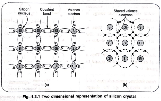
A symbolic two dimensional structure is used to represent a three dimensional
crystal form, as shown in Fig. 1.3.1 (a).
•
The covalent bonds are represented by a pair of dotted lines encircling the two
electrons forming the covalent bond. The more clear understanding of the
covalent bonds can be obtained from Fig. 1.3.1 (b) which shows the sharing of
valence electrons.
•
Both the electrons are shared by the two atoms. Hence the outermost shell of
all the atoms is completely filled, and the valence electrons are tightly bound
to the parent atoms.
• No free electrons are available at absolute zero temperature. Hence such an intrinsic semiconductor behaves as a perfect insulator at absolute zero temperature.
2. Thermal Generation in Intrinsic Semiconductors
•
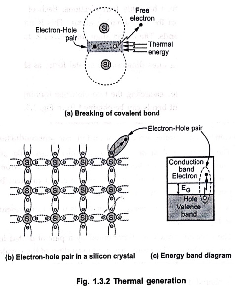
At room temperature, the number of valence electrons absorb the thermal energy,
due to which they break the covalent bond and drift to the conduction band.
Such electrons become free to move in the crystal as shown in Fig. 1.3.2 (a).
•
Once the electrons are dislodged from the covalent bonds, then they become
free. Such free electrons wander in a random fashion in a crystal.
•
The energy required to break a covalent bond is 0.72 eV for germanium and 1.1
eV for silicon, at room temperature.
•
When a valence electron drift from valence to conduction band breaking a
covalent bond, a vacancy is created in the broken covalent bond. Such a vacancy
is called a hole. Whenever an electron becomes free, the corresponding hole
gets generated.
•
So free electrons and holes get
generated in pairs. The formation of electron‒hole pair is shown in Fig.
1.3.2 (b) while the corresponding energy band diagram is shown in Fig. 1.3.2
(c). Such a generation of electron hole pairs due to thermal energy is called thermal generation.
•
The concentration of free electrons and holes is always equal in an intrinsic
semiconductor. The hole also serves as a carrier of electricity similar to that
of free electron.
•
An electron is negatively charged particle. Thus a hole getting created due to
electron drift is said to be positively charged.
Key
Point: Thus in an intrinsic semiconductors both holes as
well as free electrons are the charge carriers.
3. Conduction in Intrinsic Semiconductors
•
When a battery is connected to a semiconductor, free electrons move towards
positive of battery and constitute a current called an electron current. The
free electrons move in conduction band.
•
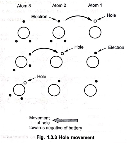
Consider three atoms as shown in Fig. 1.3.3.
•
There is a hole in atom 1. When battery is applied, electron from atom 2 shifts
into hole of atom 1, creating hole in atom 2.
•
Then electron from atom 3 shifts into hole of atom 2 creating hole in atom 3.
•
Thus hole moves from atom 1 to atom 3 and like this it gets attracted towards
negative of battery.
•
As holes are positively charged, movement of hole constitutes a current called
hole current. The holes to always move in valence band.
•
In semiconductors, the total current is combination of electron current and
hole current.
•
The direction of conventional current is always opposite to the direction of
free electrons i.e. from positive to negative of battery, external to the battery.
Key
Point: The current due to movement of free electrons in
the conduction band is an electron current. The current due to movement of
holes in the valence band is a hole current. The electron as well as hole
current together constitutes current in an intrinsic semiconductor.
Total current = Electron current +
Hole current
4. Conductivity of Intrinsic Semiconductor
•
The property called conductivity indicates the ease with which a material can
carry the current. Thus more conductivity means that material can carry high
current, very easily.
•
The conductivity of a good conductor is high while that of an insulator is low.
•
In intrinsic semiconductor, very few electron‒hole pairs get generated at room
temperature. Hence very small current can be constituted, due to the
application of voltage to an intrinsic semiconductor.
•
Thus the conductivity of an intrinsic semiconductor at room temperature is very
low. Such a low conductivity has very little practical significance.
Key
Point: Due to low conductivity, the intrinsic
semiconductors are not used used in practice for manufacturing of electronic
devices.
5. Recombination of Electrons and Holes
•
The movement of holes in the valence band is always random and similarly the
movement of free electrons in the conduction band is also random.
•
Thermal agitation continues to produce new hole‒electron pairs.
•
Occasionally, a free electron approaches a hole and falls into it. This merging
of a free electron and a hole is called recombination.
•
After the recombination, an electron‒hole pair gets disappeared.
•
Due to recombination the number of charge carriers decreases.
•
The amount of time between the creation
and disappearence of a free electron or hole is called the mean life time of
the charge carrier.
•
At any temperature, at any instant, the free electrons and holes, the two types
of charge carriers are present in equal numbers. This concentration is called
intrinsic concentration. Mathematically this is indicated as,
n = p = ni;
where
volume
n
= Number of free electrons per unit
p
= Number of holes per unit volume
ni
= Intrinsic concentration.
•
The concentration is measured in the units number per m3 or per cm3.
6. Energy Band Diagram for Intrinsic Semiconductor
•
In the energy band diagram of semiconductors, the probability of occupancy of
an energy level by an electron is indicated by a level called fermilevel
denoted as EF.
•
In intrinsic semiconductors, the number of electrons and holes are always equal
in number.
•
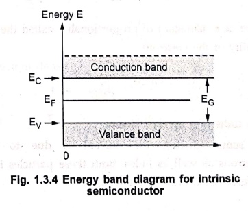
If Ec is the lowest energy level of conduction band and EV is the
highest energy level of valence band then the probability of finding electron
in conduction band and probability of finding hole in valence band is same.
•
Hence the fermilevel in such a case lies exactly at the centre of forbidden
energy band and given by
EF
= [ Ec + Ev ] / 2
•
Thus energy band diagram for intrinsic semiconductor is as shown in Fig. 1.3.4.
Review Questions
1. Explain intrinsic semiconductor.
2. Explain generation of electron‒hole pairs in an intrinsic
semiconductor.
3. Explain how conduction takes place in an intrinsic
semiconductor.
4. Describe the generation and recombination of charge carriers
in intrinsic semiconductors.
Electron Devices: Chapter 1: Semiconductor : Tag: electronics : Crystal Structure, Thermal Generation, Conduction, Conductivity, Energy Band Diagram - Intrinsic Semiconductors
Electron Devices: Chapter 1: Semiconductor
Under Subject

Electron Devices
EC25C01 2nd Semester ECE Dept | 2025 Regulation | 2nd Semester 2025 Regulation
Related Subjects

English Essentials II
EN25C02 2nd Semester | 2025 Regulation | 2nd Semester 2025 Regulation

Tamils and Technology தமிழர்களும் தொழில்நுட்பமும்
UC25H02 2nd Semester | 2025 Regulation | 2nd Semester 2025 Regulation

Linear Algebra
MA25C02 2nd Semester | 2025 Regulation
Electron Devices
EC25C01 2nd Semester ECE Dept | 2025 Regulation | 2nd Semester 2025 Regulation

Data Structures using CPlusPlus
CS25C05 2nd Semester ECE Dept | 2025 Regulation | 2nd Semester 2025 Regulation

Circuits and Network Analysis
EC25C02 2nd Semester ECE Dept | 2025 Regulation | 2nd Semester 2025 Regulation

Re-Engineering for Innovation
ME25C05 2nd Semester | 2025 Regulation | 2nd Semester 2025 Regulation

Engineering Drawing - Laboratory
ME25C01 2nd Semester | 2025 Regulation | 2nd Semester 2025 Regulation

Data Structures using CPlusPlus - Laboratory
CS25C05 2nd Semester ECE Dept | 2025 Regulation | 2nd Semester 2025 Regulation

Devices and Circuits Laboratory
EC25C03 2nd Semester ECE Dept | 2025 Regulation | 2nd Semester 2025 Regulation