Electron Devices: Chapter 1: Semiconductor
Diffusion Current and Diffusion Current Density
Semiconductor
Questions: 1. What is diffusion current? Derive the expressions for the diffusion current densities. 2. Explain Einstein's relationship and voltage equivalent of temperature. 3. Define mean life time and diffusion length for the charge carriers.4. Important Example Solved Problems
Diffusion
Current and Diffusion Current Density
•
This is the current which is due to the transport of charges occurring because
of nonuniform concentration of charged particles in a semiconductor.
•
Consider a piece of semiconductor which is nonuniformly doped. Due to such
nonuniform doping, one type of charge carriers occur at one end of a piece of
semiconductor.
•
The charge carriers are either electrons or holes, of one type depending upon
the impurity used. They have the same polarity and hence experience a force of
repulsion between them.
•
The result is that there is a tendency of the charge carriers to move gradually
i.e. to diffuse from the region of high carrier density to the low carrier
density. This process is called diffusion.
•
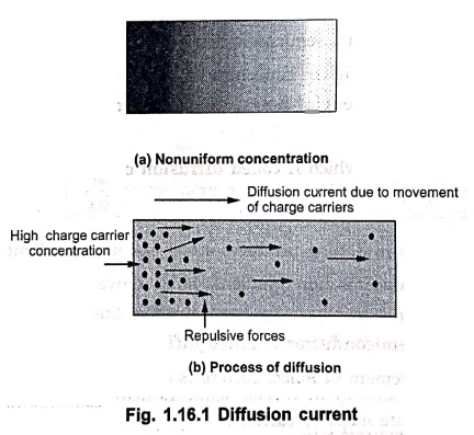
This movement of charge carriers under the process of diffusion constitutes a
current called diffusion current. This is shown in Fig. 1.16.1.
•
The diffusion current continues till all the carriers are evenly distributed
throughout the material.
•
A diffusion current is possible only in case of nonuniformly doped
semiconductors while drift current is possible in semiconductors as well as
conductors.
Key
Point: The diffusion current exists without external
voltage applied while drift current can not exist without an external voltage
applied.
1. Concentration Gradient
•
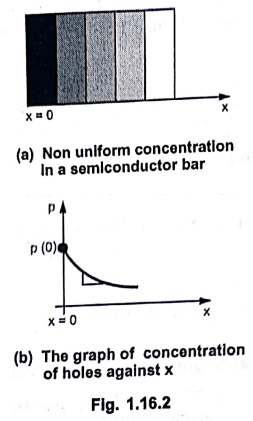
Consider a p‒type semiconductor bar which is nonuniformly doped along its
length, in the direction of x as shown in Fig. 1.16.2 (a). As x increases, the
doping concentration decreases.
•
To form p‒type of semiconductor, acceptor impurity is added which creates holes
as the majority charged particles.
•
Let P be the concentration of holes, but due to nonuniform doping it is not
constant but is changing with respect to x.
•
Let concentration of holes at x = 0 is p = p(0) and is maximum as bar is
heavily doped at x = 0. As x increases, the concentration of holes decreases.
The nature of the variation in p against distance x is shown in Fig. 1.16.2
(b).
•
The slope of the graph can be observed from Fig. 1.16.2 (b) is the ratio of
change in concentration to change in distance. It is called rate of change of
concentration or concentration gradient.
Slope of graph = Concentration gradient = dp/dx
….. (1.16.1)
•
Hence nonuniform doping produces a concentration gradient in a semiconductor.
•
Due to such concentration gradient, holes move from the higher concentration
area to the lower concentration area to adjust the concentration. Such a
movement of holes, due to the concentration gradient in a semiconductor is
called diffusion.
•
Due to the movement of holes, current is constituted in a bar which is called diffusion
current.
•
There exists such a diffusion current in n‒type semiconductor if it is
nonuniformly doped, due to movement of electrons which are majority carriers.
Key
Point: Nonuniform doping creats concentration gradient, due
to which diffusion of charge carriers exists.
2. Diffusion Current Density
•
Consider a nonuniformly doped p‒type semiconductor bar as shown in Fig. 1.16.2
(a).
•
The diffusion current density is proportional to the concentration gradient,
which is responsible for the diffusion and hence the diffusion current.
Jp ∝
dp/dx
where Jp Diffusion current density due to
holes
•
Hence the diffusion current density is expressed by,
Jp = q Dp dp/dx
where Dp = Diffusion constant for
holes expressed in square metres per second. (m2/sec).
Key
Point: The current due to holes is in the direction of
the conventional current and hence treated as positive. But slope of the graph
i.e. dp/dx is negative giving the negative diffusion current density for holes.
But to get positive sign for holes, an additional negative sign is used to
compensate for negative sign of dp/dx. Hence diffusion current density for
holes is mathematically expressed as,
Jp = ‒ q Dp dp/dx
•
In case of n‒type bar, such diffusion current is due to the electrons. Current
due to the electrons is in opposite direction to the conventional current and
mathematically treated to be negative. The concentration gradient dn/dx is
negative where n is concentration of electrons.
•
Hence diffusion current density to electrons is expressed by,
Jp = + q Dn dn/dx
where
Dn = Diffusion constant for electrons in square metres per second (m2/sec).
•
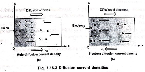
Fig. 1.16.3 (a) shows the direction of diffusion of holes and corresponding
diffusion current density. Fig. 1.16.3 (b) shows the direction of diffusion of
electrons and corresponding diffusion current density.
•
Observe that the charge carriers whether it is hole or electron, always move
from high concentration area towards low concentration area. Hence direction of
diffusion is same in both the cases. But resulting current densities have
opposite directions.
3. Total Current Density Due to Drift and Diffusion
•
We have seen that the drift current is due to the applied voltage while the
diffusion current is due to the concentration gradient.
•
But in semiconductor it is very much possible that both the types of currents
may exist simultaneously.
•
In practice in such situation there exists four components of current as the
drift current due to electrons and due to holes, while the diffusion current
due to electrons and due to holes.
•
Drift current density for electrons and holes can be expressed as,
Jn = n q μn E and Jp
= P q μp E
•
Diffusion current density due to the electrons and holes can be expressed from
equations (1.16.3) and (1.16.4) as,
Jn = + q Dn dn/dx and Jp
= ‒ q Dp dp/dx
Total
current density due to the electrons can be expressed as,
Jn = n q μn
E + q Dn dn/dx
Total
current density due to the holes can be expressed as,
Jp = P q μp
E ‒ q Dp dp/dx
And
hence the total current density due to the electrons and holes (Drift +
Diffusion) is,
J = Jn +Jp
4. Einstein's Relationship
•
It is now known that drift current density is proportional to the mobility (μ)
while diffusion current density is proportional to the diffusion constant (D).
There exists a fixed relation between these two constants which is called Einstein's relation.
•
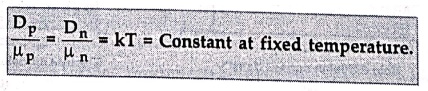
It states that, at a fixed temperature, the ratio of diffusion constant to the
mobility is constant. This is Einstein's relation. Mathematically it is
expressed as,
DP/μP = Dn / μn
= kT = Constant at fixed temperature.
……….. (1.16.8)
where
T is the temperature in °K and k is the Boltzmann's constant = 8.62 × 10‒5
eV/°K
5. Voltage Equivalent of Temperature
•
In the equation (1.16.8), the product kT is called voltage equivalent of
temperature.
•
The voltage equivalent of temperature is denoted by VT.
VT = KT = Voltage equivalent of
temperature
……….. (1.16.9)
At
room temperature i.e. at 27 °C,
T
= 273 + 27 = 300 °K
VT = kT = 8.62 × 10‒5 ×
300 = 0.02586 V ≈ 26 mV at 300 °K
Key
Point: The value of VT = 26 mV at 27° C i.e.
300 °K is very commonly used while solving the examples.
•
Substituting this in equation (1.16.8) we get,
Dn / μn = Dp /
μp = VT = 0.02586 at room temperature
μn=39 Dn and μp=39
DP at room temperature.
………..
(1.16.10)
•
In general we can express the relation between mobility and diffusion constant
as,
μ = 39 D at room temperature
……. (1.16.11)
6. Carrier Lifetimes
•
In a pure semiconductor the number of free electrons is always equal to number
of holes. The thermal agitation continues to produce new hole‒electron pairs
while previous pairs disappear. This disappearing of pairs is due to the
process called recombination.
•
The merging of a free electron and hole is called recombination.
•
The amount of time between the creation and disappearence of a free electron
and hole pair is called its lifetime.
•
Thus a hole exists for τP seconds before it recombines while a free
electron exists for τn seconds before it recombines. τP
and τn are called carrier lifetimes of hole and electron
respectively.
•
Carrier lifetime is also called mean lifetime of the hole and electron. Carrier
lifetimes range from nanoseconds to hundreds of microseconds.
Diffusion Lenth L
Let
τn
= Mean life time of free electron
τP
= Mean life time of free hole.
•
After recombination, these charge carriers vanish and concentration decreases
exponentially with distance.
Key
Point: The average distance covered by an excess charge
carrier while diffusion during its life time is called diffusion length of that
charge carrier. It is denoted by L.
Ln = Diffusion length of free
electron
Lp = Diffusion length of free hole.
•
The diffusion length L is related to main life time τ through the diffusion
constant D of the charge carrier. Mathematically this relationship is given by,
L = √(Dτ)
Thus,
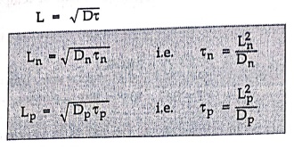
Ln = √(Dnτn)
Lp = √(Dpτp)
τn = Ln2
/ Dn
τp = LP2
/ DP
Ex. 1.16.1 Find out the diffusion constant of
holes if their mobility is given as 0.039 m2/v‒sec.
Solution:
μp = 0.039 m2/V‒s
According
to Einstein's relation, Dp / μр = KT
At 300 °K,
Dp
/ μр = Dp / 0.039 = 26 × 10‒3
i.e.
Dp = 1.01 × 10‒3
Ex. 1.16.2 The phosphrous (donor)
concentration in a region of a silicon crystal varies linearly from a
concentration of n0 = 1014 cm‒3 at x = 0 mm to
a concentration of n1 = 1017 cm-3 at x = 1 mm.
The diffusion constant for electrons is
Dn = 22.5 cm2/s, the diffusion constant for holes
is Dp = 5.2 cm2/s and the temperature is 300 °K. What is
the diffusion current density in the
positive x‒direction?
Solution:
n0 = 1014 cm-3
n1 = 1017 cm-3,
x1
= 1 mm,
x0
= 0 mm,
Dn = 22.5 × 10⁻⁴ m2/s,
Dp
= 5.2 × 10⁻⁴ m2/s.
For
silicon, ni = 1.5 × 1010 cm‒3
ni2 = np
... Law of mass action
P0 = ni2 / n0
= (1.5×10¹⁰)2 / 1014 = 2.15 × 10⁶
cm-3
P1
= ni2 / n1 = (1.5×10¹⁰)2
/ 1017 = 2.15 × 103 cm-3
dp/dx
= [P1‒P0] / [x1‒x0] = [ 2.25×10³
‒ 2.25×10⁶] / 10‒1 = ‒2.248 × 107 cm‒4
dn/dx = [n1‒n0] / [x1‒x0]
= [1017 ‒ 1014] / 10‒1 = 9.99 × 10¹⁷
cm‒4
J = Jn + Jp = [ qDn
dn/dx ] ‒ [ qDp dp/dx ]
=
1.602×10‒19 [ 22.5×9.99×1017 ‒ 5.2×(‒2.248×10⁷)]
=
3.6 A/cm2
=
3.6×10⁴ A/m2
Review Questions
1. What is diffusion current? Derive the expressions for the
diffusion current densities.
2. Explain Einstein's relationship and voltage equivalent of
temperature.
3. Define mean life time and diffusion length for the charge
carriers.
Electron Devices: Chapter 1: Semiconductor : Tag: electronics : Semiconductor - Diffusion Current and Diffusion Current Density
Electron Devices: Chapter 1: Semiconductor
Under Subject

Electron Devices
EC25C01 2nd Semester ECE Dept | 2025 Regulation | 2nd Semester 2025 Regulation
Related Subjects

English Essentials II
EN25C02 2nd Semester | 2025 Regulation | 2nd Semester 2025 Regulation

Tamils and Technology தமிழர்களும் தொழில்நுட்பமும்
UC25H02 2nd Semester | 2025 Regulation | 2nd Semester 2025 Regulation

Linear Algebra
MA25C02 2nd Semester | 2025 Regulation
Electron Devices
EC25C01 2nd Semester ECE Dept | 2025 Regulation | 2nd Semester 2025 Regulation

Data Structures using CPlusPlus
CS25C05 2nd Semester ECE Dept | 2025 Regulation | 2nd Semester 2025 Regulation

Circuits and Network Analysis
EC25C02 2nd Semester ECE Dept | 2025 Regulation | 2nd Semester 2025 Regulation

Re-Engineering for Innovation
ME25C05 2nd Semester | 2025 Regulation | 2nd Semester 2025 Regulation

Engineering Drawing - Laboratory
ME25C01 2nd Semester | 2025 Regulation | 2nd Semester 2025 Regulation

Data Structures using CPlusPlus - Laboratory
CS25C05 2nd Semester ECE Dept | 2025 Regulation | 2nd Semester 2025 Regulation

Devices and Circuits Laboratory
EC25C03 2nd Semester ECE Dept | 2025 Regulation | 2nd Semester 2025 Regulation