Electron Devices: Chapter 1: Semiconductor
Introduction of Semiconductor
Question 1. Explain the classification of materials based on energy band diagram. 2. Semiconductor: Energy Bands 3. Structure of Silicon and Germanium
Electron
Devices
Chapter
1: Semiconductor
Introduction
•
The smallest particle of matter is an atom which is made up of three
fundamental particles,
i)
Neutron
ii)
Proton
iii)
Electron
•
The proton is positively charged, an electron is negatively charged while the
neutron is uncharged, i.e. electrically neutral.
•
According to to Bohr's theory, the atoms planetary type structure. All protons
and neutrons are bound together at the centre of an atom which is nucleus.
•
The electrons revolve around the nucleus in different orbits or shells. Each
shell contains maximum number of 2n2 electrons where n is number of
shell. The exception to this is that the last shell contains maximum 8 electrons
irrespective of its number.
•
The electrons in the first orbit are closest to the nucleus and under
tremendous force of attraction by the nucleus.
•
The last shell electrons are loosely bound to the nucleus. Such shell is called
valence shell and electrons in this shell are called valence electrons.
•
Each shell has energy level associated with it. The energy level of first shell
is lowest and that of last shell is highest.
•
When atom absorbs energy from heat or light, the electrons in valence shell
absorb this energy and become free from the attraction of nucleus. Such
electrons are called free electrons and are responsible for the conduction.
More the number of free electrons, better is the conductivity.
Energy Bands
•
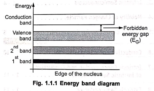
The energy levels of electrons in each orbit merge into each other to form an
energy band.
•
The energy levels of valence electrons merge into each other to form a valence
band.
•
When a valence electron absorbs energy, it becomes free electron. The energy
levels of all the free electrons merge into each other conduction band.
•
An energy band which separates the conduction band and the valence band is
called forbidden band or forbidden gap.
•
The electrons in valence band are still under the force of attraction of
nucleus. The electrons in the conduction band are free electrons which are free
from the force of attraction of nucleus.
•
No electron exists in the forbidden band. The energy difference between energy
of conduction band and valence band is called forbidden gap energy denoted as EG.
•
This EG represents amount of energy required to be given to
electrons of valence band to transfer them to the conduction band.
•
The graphical representation of energy bands is called energy band diagram
which is shown in Fig. 1.1.1.
•
The energy gap EG is measured in the unit electron‒volt (eV).
Classification based on Energy Band Diagram
•
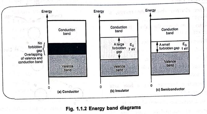
Based on energy gap EG the materials are classified as conductors,
insulators and semiconductors.
•
In conductors, large number of free electrons exist at normal room temperature.
So EG does not exist. The valence and conduction bands are
overlapped. This is shown in Fig. 1.1.2 (a). The examples are copper,
aluminium, silver etc.
•
In insulators, the EG is very high about 7 eV. Hence at very high
voltage or temperature also, the electrons cannot move from valence to
conduction band. Hence these materials can not conduct at all and called
insulators. This is shown in Fig. 1.1.2 (b). The examples are wood, mica, paper
etc.
• In semiconductors, at absolute zero temperature. (‒273 °C), the conduction band is empty and they behave like perfect insulators. The energy gap EG is about 1 eV. At normal temperature, some electrons move from valence to conduction band hence few free electrons are available. Hence materials can conduct partially. At room temperature EG = 1.12 eV for silicon and 0.78 eV for germanium. As temperature increases the EG decreases and large number of free electrons are available. This is shown in Fig. 1.1.2 (c). The examples are silicon and germanium.
Structure of Silicon and Germanium
•
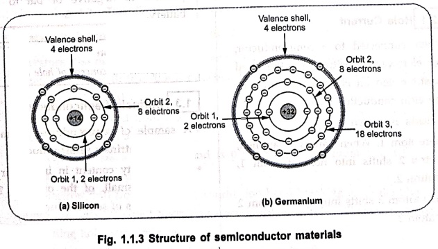
The atomic number of silicon is 14 while that of germanium is 32.
•
Fig. 1.1.3 (a) shows the structure of silicon while Fig. 1.1.3 (b) shows the
structure of germanium.
•
In both the materials, there are 4 valence electrons.
Review
Question
1. Explain the classification of materials based on energy band
diagram.
Electron Devices: Chapter 1: Semiconductor : Tag: electronics : - Introduction of Semiconductor
Electron Devices: Chapter 1: Semiconductor
Under Subject

Electron Devices
EC25C01 2nd Semester ECE Dept | 2025 Regulation | 2nd Semester 2025 Regulation
Related Subjects

English Essentials II
EN25C02 2nd Semester | 2025 Regulation | 2nd Semester 2025 Regulation

Tamils and Technology தமிழர்களும் தொழில்நுட்பமும்
UC25H02 2nd Semester | 2025 Regulation | 2nd Semester 2025 Regulation

Linear Algebra
MA25C02 2nd Semester | 2025 Regulation
Electron Devices
EC25C01 2nd Semester ECE Dept | 2025 Regulation | 2nd Semester 2025 Regulation

Data Structures using CPlusPlus
CS25C05 2nd Semester ECE Dept | 2025 Regulation | 2nd Semester 2025 Regulation

Circuits and Network Analysis
EC25C02 2nd Semester ECE Dept | 2025 Regulation | 2nd Semester 2025 Regulation

Re-Engineering for Innovation
ME25C05 2nd Semester | 2025 Regulation | 2nd Semester 2025 Regulation

Engineering Drawing - Laboratory
ME25C01 2nd Semester | 2025 Regulation | 2nd Semester 2025 Regulation

Data Structures using CPlusPlus - Laboratory
CS25C05 2nd Semester ECE Dept | 2025 Regulation | 2nd Semester 2025 Regulation

Devices and Circuits Laboratory
EC25C03 2nd Semester ECE Dept | 2025 Regulation | 2nd Semester 2025 Regulation