Electron Devices: Chapter 1: Semiconductor
Semiconductor: Two Marks Important Questions and Answers
Electron Devices
Electron Devices: Chapter 1: Semiconductor: Anna University Part A Two Marks Important Questions and Answers
Electron
Devices
Chapter
1: Semiconductor
Two Marks Important Questions and Answers
1. Why silicon is widely
used than germanium ?
Looking
at the structure of silicon and germanium atom, it can be seen that valence
shell of silicon is 3rd shell while valence shell of germanium is 4th shell.
Hence valence electrons of germanium are at larger distance from nucleus than
valence electrons of silicon. Hence valence electrons of germanium are more
loosely bound to the nucleus than those of silicon. Thus valence electrons of
germanium can easily escape from the atom, due to very small additional energy
imparted to them. So at high temperature, germanium becomes unstable than
silicon and hence silicon is widely used semiconductor material.
2. Find forbidden energy
gap for germanium and silicon at 40°C.
T
= 40 °C = 313 °K
For
Si,
EG
= 1.21 ‒ 3.6 × 10‒4 × T
= 1.21 ‒ 3.6×10‒4 × 313 = 1.097eV
For
Ge,
EG
= 0.785 ‒ 2.23 × 10‒4 × T
=
0.785 ‒2.23 × 10‒4 × 313
=
0.7152 eV
3. Define one
electron‒volt.
The
energy required by an electron to fall through a potential of one volt is
called one electron‒volt (eV).
1 eV = 1.6 × 10‒19 J
4. What is intrinsic
semiconductor?
A
sample of semiconductor in its purest form is called an intrinsic
semiconductor. The impurity content in an intrinsic semiconductor is very very
small, of the order of one part in 100 million parts of semiconductor.
5. Why the intrinsic
semiconductors are not used in practice for manufacturing of electronic devices
?
In
intrinsic semiconductor, very few electron‒hole pairs pairs get generated at
room temperature. Hence very small current can be constituted, due to the
application of voltage to an intrinsic semiconductor. Thus the conductivity of
an intrinsic semiconductor at room temperature is very low. Such a low
conductivity has very little practical significance.
Hence
the intrinsic semiconductors are not used for the manufacturing of electronic
devices.
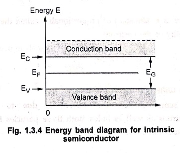
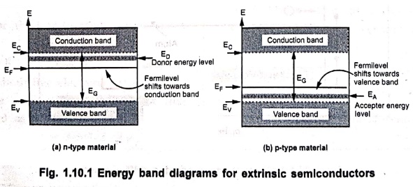
6. Draw the energy band
diagram for intrinsic and extrinsic semiconductors.
7. What is diffusion
current in PN junction diode ?
When
a semiconductor is nonuniformly doped, then there exists concentration
gradient. On one side there is high carrier concentration while on the other
there is low carrier concentration. Due to this, charges start moving from
higher to lower concentration area. This process is called diffusion. When the
charges move charges move due to diffusion, the current gets established in a
semiconductor which is called a diffusion current.
8. Define drift and
diffusion current.
When
a voltage is applied to a material, the free electrons move towards the
positive of the battery. While moving they collide with the adjacent atoms and
keep changing their directions randomly. Still they keep drifting towards the
positive of the battery. This is called drifting of charge carriers and the
current due to such drifting of charge carriers is called drift current.
In
case of diffusion current, the external voltage is not required. Due to
nonuniform doping of the material, a concentration gradient is created across
the material due to which the charge carriers move from higher to lower
concentration area. This is called diffusion and the corresponding current is
called diffusion current.
9. Name some donor and
acceptor impurities.
The
donor impurities are arsenic, bismuth, phosphorous while acceptor impurities
are gallium, indium and boron.
10. What is the value of VT
(Volt equivalent of temperature) at a temperature of 300 °K?
VT
= KT = 8.62 × 10‒5 × (300) = 0.02586 V
11. Define mass action law.
If
n is the concentration of free electrons and P is the concentration of holes
then the law of mass action states that the product of concentrations of
electrons and holes is always constant, at a fixed temperature.
Mathematically
it is expressed as,
Np = ni2 where ni
is intrinsic concentration
12. Consider a silicon pn
junction at T = 300 ° K so that n1 = 1.5×1010 cm‒3.
The n type doping is 1× 1016 cm‒3 and a forward bias of
0.60 V is applied to the pn junction. Calculate the minority hole concentration
at the edge of the space charge region.
The
hole concentration at the edge of the space charge region is,
Pn = Pn0 eV/VT
…….Refer equation (1.18.8)
Pn0
= ni2 / ND = (1.5×10¹⁶)2
/ 1×10²²
Pn
= 2.25 × 10¹⁰ e0.6/0.0259
= 2.588 × 10²⁰ /m3
Note
that ni = 1.5 × 10¹⁰ / cm3 = 1.5 × 10¹⁶
/ m3
13. Consider a gallium
arsenide sample at T = 300 K with doping concentration of Na=0, Nd=1016
cm‒3 and μn = 8500. Calculate the drift current density
if the applied electric field is E = 10 V/cm.
Nd=1016
cm‒3
μn
= 8500,
E
= 10 V/cm.
J = Nd μn qE
=
1016 × 8500 × 1.6 × 10‒19 × 10
J = 136 A/cm2
Electron Devices: Chapter 1: Semiconductor : Tag: electronics : Electron Devices - Semiconductor: Two Marks Important Questions and Answers
Electron Devices: Chapter 1: Semiconductor
Under Subject

Electron Devices
EC25C01 2nd Semester ECE Dept | 2025 Regulation | 2nd Semester 2025 Regulation
Related Subjects

English Essentials II
EN25C02 2nd Semester | 2025 Regulation | 2nd Semester 2025 Regulation

Tamils and Technology தமிழர்களும் தொழில்நுட்பமும்
UC25H02 2nd Semester | 2025 Regulation | 2nd Semester 2025 Regulation

Linear Algebra
MA25C02 2nd Semester | 2025 Regulation
Electron Devices
EC25C01 2nd Semester ECE Dept | 2025 Regulation | 2nd Semester 2025 Regulation

Data Structures using CPlusPlus
CS25C05 2nd Semester ECE Dept | 2025 Regulation | 2nd Semester 2025 Regulation

Circuits and Network Analysis
EC25C02 2nd Semester ECE Dept | 2025 Regulation | 2nd Semester 2025 Regulation

Re-Engineering for Innovation
ME25C05 2nd Semester | 2025 Regulation | 2nd Semester 2025 Regulation

Engineering Drawing - Laboratory
ME25C01 2nd Semester | 2025 Regulation | 2nd Semester 2025 Regulation

Data Structures using CPlusPlus - Laboratory
CS25C05 2nd Semester ECE Dept | 2025 Regulation | 2nd Semester 2025 Regulation

Devices and Circuits Laboratory
EC25C03 2nd Semester ECE Dept | 2025 Regulation | 2nd Semester 2025 Regulation