Electron Devices: Chapter 1: Semiconductor
Formation of Extrinsic Semiconductor Materials
Questions: 1. Explain the formation of n‒type material and conduction in n‒type material. 2. Explain the following: i) Formation of p‒type semiconductor. ii) Conduction in p‒type material.
Formation
of Extrinsic Semiconductor Materials
It
is seen that when pentavalent impurity, is added to intrinsic semiconductor, n‒type
extrinsic semiconductor is obtained. While when trivalent impurity is added to
intrinsic semiconductor, p‒type extrinsic semiconductor is obtained.
1. Formation of n‒type Semiconductor
•
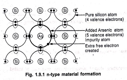
Consider a pentavalent impurity like Arsenic (As) is added to Silicon (Si). It
is a donor impurity with five valence electrons.
•
The arsenic atom fits in the silicon crystal in such a way that its four
valence electrons form covalent bonds with four adjacent silicon atoms.
Remember that both germanium and silicon have four electrons in the valence
shell.
•
The fifth electron of arsenic has no chance to form covalent bond hence this
electron enters in conduction band as a free electron. Thus each As atom added
to Si atom donates one free electron. This is shown in Fig. 1.9.1.
•
The number of free electrons can be controlled by the amount of impurity added.
•
Since the free electrons have negative charges, the material obtained is called
n‒type extrinsic semiconductor.
2. Conduction in n‒type Material
•
In intrinsic semiconductor, the number of free electrons and holes is same. But
when pentavalent impurity is added in large extent, the number of free
electrons becomes very high compared to the number of holes.
•
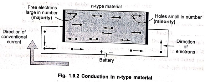
Thus if voltage is applied, the current is mainly because of free electrons
which are large in number.
Hence
the free electrons are called majority carriers in n‒type material. While there
is small current due to less number of holes. Hence the holes are called minority
carriers in n‒type material.
•
This is shown in Fig. 1.9.2.
3. Formation of p‒type Semiconductor
•
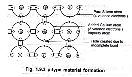
Consider a trivalent impurity like Gallium (Ga) is (4 valence electrons) added
to Silicon (Si). It is an acceptor impurity with three valence electrons.
•
The gallium atom fits into the silicon crystal in such a way that its three
valence electrons form covalent bonds with the three adjacent silicon atoms.
There is shortage of one electron to form a covalent bond. This creates a
vacancy in the fourth covalent bond which is nothing but a hole. Thus each Ga
atom added into Si atom creates one hole which is ready to accept an electron.
This is shown in Fig. 1.9.3.
• The number of such holes can be controlled by the amount of impurity added to the silicon.
•
As the holes are treated as positively charged, the material obtained is called
p‒type extrinsic semiconductor.
4. Conduction in p‒type Material
•
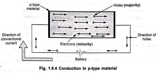
When large trivalent impurity is added to silicon or germanium, the number of
holes becomes very high as compared to free electrons.
•
Thus if voltage is applied, the holes which are large in number move towards
negative of battery and mainly responsible for the current. Hence the hole are
called majority carriers in p‒type material while there is small current due to
the movement of less number of free electrons. Hence the free electrons are
called minority carriers in p‒type material.
•
This is shown in Fig. 1.9.4.
Review
Questions
1. Explain the formation of n‒type material and conduction in n‒type
material.
2. Explain the following:
i) Formation of p‒type semiconductor.
ii) Conduction in p‒type material.
Electron Devices: Chapter 1: Semiconductor : Tag: electronics : - Formation of Extrinsic Semiconductor Materials
Electron Devices: Chapter 1: Semiconductor
Under Subject

Electron Devices
EC25C01 2nd Semester ECE Dept | 2025 Regulation | 2nd Semester 2025 Regulation
Related Subjects

English Essentials II
EN25C02 2nd Semester | 2025 Regulation | 2nd Semester 2025 Regulation

Tamils and Technology தமிழர்களும் தொழில்நுட்பமும்
UC25H02 2nd Semester | 2025 Regulation | 2nd Semester 2025 Regulation

Linear Algebra
MA25C02 2nd Semester | 2025 Regulation
Electron Devices
EC25C01 2nd Semester ECE Dept | 2025 Regulation | 2nd Semester 2025 Regulation

Data Structures using CPlusPlus
CS25C05 2nd Semester ECE Dept | 2025 Regulation | 2nd Semester 2025 Regulation

Circuits and Network Analysis
EC25C02 2nd Semester ECE Dept | 2025 Regulation | 2nd Semester 2025 Regulation

Re-Engineering for Innovation
ME25C05 2nd Semester | 2025 Regulation | 2nd Semester 2025 Regulation

Engineering Drawing - Laboratory
ME25C01 2nd Semester | 2025 Regulation | 2nd Semester 2025 Regulation

Data Structures using CPlusPlus - Laboratory
CS25C05 2nd Semester ECE Dept | 2025 Regulation | 2nd Semester 2025 Regulation

Devices and Circuits Laboratory
EC25C03 2nd Semester ECE Dept | 2025 Regulation | 2nd Semester 2025 Regulation