Electron Devices: Chapter 1: Semiconductor
Potential Variation in a Continuously Graded Semiconductor
Questions: 1. Derive the expression for the potential difference existing in a continuously graded semiconductor. 2. Explain the law of junction. Hence prove the law of mass action from it. 3. Important Example Solved Problems
Potential
Variation in a Continuously Graded Semiconductor
•
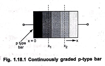
Consider a p‒type continuously graded bar i.e. nonuniformly doped bar as shown
in Fig. 1.18.1.
•
No external voltage is applied to the bar. The bar is open circuited. As no
external voltage is applied and it is open circuited, net current through the bar
is zero.
•
But due to the nonuniform doping there exists a diffusion current as holes move
from high concentration to low concentration area. Hence there exists a
diffusion current density of,
Jp = ‒q Dp dp/dx
………. (1.18.1)
•
But as bar is open circuited, net current through it is zero.
•
This means there exists one more internal current which is equal to diffusion
current but in opposite direction to it. This is a drift current flowing in the
bar in opposite direction to that of diffusion current.
•
The current density of this current is,
Jp = p qμpE ……..(1.18.2)
•
But drift current cannot exist without a potential difference and applied
voltage to the bar is zero. So externally E is zero.
•
This indicates that the E required for the circulation of drift current gets
generated internally.
•
This indicates that nonuniform doping of bar results in the induced voltage.
•
And as net current through the bar is zero we can write for open circuited bar,
‒ q Dp
dp/dx + p q μp E = 0
………….(1.18.3)
1. Expression for the Potential Difference
•
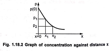
To derive the expression for the potential difference between any two points of
a nonuniformly doped bar, consider the two points at a distance of x = x1
and x = x2 as shown in Fig. 1.18.2.
•
Let concentration of holes at x = x1 is p = P1 and
concentration of holes at x = x2 is p = p2.
•
This is due to nonuniform doping and is indicated in the graph shown in Fig.
1.18.2.
•
There exists a potential difference between x1 and x2
which is responsible to circulate drift current equal and opposite to diffusion
current.
Let
potential at x1 = v1 and
potential at x2 = v2
From
the equation (1.18.3) which indicates that net current through the bar is zero,
we can write,
p q μp E = q Dp dp/dx
pE
= Dp/μp . dp/dx
…………. (1.18.4)
According
to Einstein's relation, Dp/μp is VT.
PE
= VT. dp/dx
i.e.
E = VT/P . dp/dx
…………. (1.18.5)
•
Now E is the electric field intensity generated internally. From the definition
of electric field intensity we can write,
E = ‒ dV/dx
hence
equation (1.18.5) modifies to,
‒
dv/dx = VT/P . dp/dx
i.e.
dV = ‒ VT/P dp
………. (1.18.6)
• To get the voltage generated between x1 and x2, integrate the equation (1.18.6),
V1∫V2 dV = ‒VT
P1∫P2 1/P dp
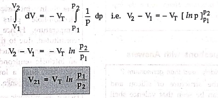
i.e.
V2 ‒ V1 = − VT [In p]P2P2
V21 = VT
In P1/P2
……..(1.18.7)
where
V21 is the potential difference between the two concentrations P1
and P2.
Key
Point: The potential difference depends on the
concentrations and not on the distance between x1 and x2.
2. Law of Junction
•
From the equation (1.18.7) we can write,
In
P1/P2 = V21/VT
i.e. P1/P2 = eV21/VT
P1
= P2 eV21/VT
and
P2
= P1 e‒V21/VT

……….(1.18.8)
•
Similarly for n‒type semiconductor bar which is nonuniformly doped, if n1
and n2 concentrations of electrons at two different points, we can
write,
n1
= n2 e‒V21/VT
and
n2
= n1 eV21/VT

……….(1.18.9)
Key
Point: There is change of sign of exponential term in
equation (1.18.9) as compared to exponential term in equations (1.18.8). This
is because diffusion current density in n‒type bar is q Dn dn/dx
which is positive.
•
The equations (1.18.8) and (1.18.9) represent law of junction.
•
Multiplying equations (1.18.8) and (1.18.9) we get,
i.e.
n1
P1 = P2 eV21/VT n2 e‒V21/VT
n1
P1 = n2 P2
•
The product of the concentrations of electrons and holes is always constant.
This
proves the law of mass action.
Review Questions
1. Derive the expression for the potential difference existing
in a continuously graded semiconductor.
2. Explain the law of junction. Hence prove the law of mass
action from it.
Electron Devices: Chapter 1: Semiconductor : Tag: electronics : - Potential Variation in a Continuously Graded Semiconductor
Electron Devices: Chapter 1: Semiconductor
Under Subject

Electron Devices
EC25C01 2nd Semester ECE Dept | 2025 Regulation | 2nd Semester 2025 Regulation
Related Subjects

English Essentials II
EN25C02 2nd Semester | 2025 Regulation | 2nd Semester 2025 Regulation

Tamils and Technology தமிழர்களும் தொழில்நுட்பமும்
UC25H02 2nd Semester | 2025 Regulation | 2nd Semester 2025 Regulation

Linear Algebra
MA25C02 2nd Semester | 2025 Regulation
Electron Devices
EC25C01 2nd Semester ECE Dept | 2025 Regulation | 2nd Semester 2025 Regulation

Data Structures using CPlusPlus
CS25C05 2nd Semester ECE Dept | 2025 Regulation | 2nd Semester 2025 Regulation

Circuits and Network Analysis
EC25C02 2nd Semester ECE Dept | 2025 Regulation | 2nd Semester 2025 Regulation

Re-Engineering for Innovation
ME25C05 2nd Semester | 2025 Regulation | 2nd Semester 2025 Regulation

Engineering Drawing - Laboratory
ME25C01 2nd Semester | 2025 Regulation | 2nd Semester 2025 Regulation

Data Structures using CPlusPlus - Laboratory
CS25C05 2nd Semester ECE Dept | 2025 Regulation | 2nd Semester 2025 Regulation

Devices and Circuits Laboratory
EC25C03 2nd Semester ECE Dept | 2025 Regulation | 2nd Semester 2025 Regulation