Electron Devices: Chapter 6: Thyristors UJT and Optoelectronic Devices
Shockley Diode
construction, Working Operation, Symbol, Characteristics, Equivalent Circuit, Application, Example Solved Problems

Questions: 1. Explain the construction and working of Shockley diode. 2. Draw and explain the characteristics of Shockley diode stating its applications.
Electron
Devices
Chapter 6: Thyristors,
UJT and Optoelectronic Devices
Shockley
Diode
•
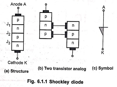
The Shockley diode is a thyristor. It has two terminals, the anode and the
cathode and four semiconductor layers. Fig. 6.1.1 (a) shows the basic
construction showing p‒n‒p‒n structure and three junctions of Shockley diode.
The Fig. 6.1.1 (b) shows the two transistor analogy while Fig. 6.1.1 (c) shows
the symbol of the Shockley diode.
•
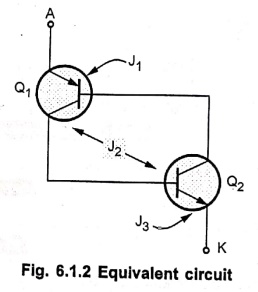
Fig. 6.1.2 shows the equivalent circuit of the Shockly diode using two
transistors. The collector of Q1 and base of Q2 are
connected. J1 is emitter base junction of Q1. J2
is the common connected base collector junction between Q1 and Q2.
J3 is base emitter junction of Q2. For the linear
operation, J1 and J3 must be forward biased as the base
emitter junctions while the junction J2 must be reverse biased as
collector base junction.
Basic Operation
•
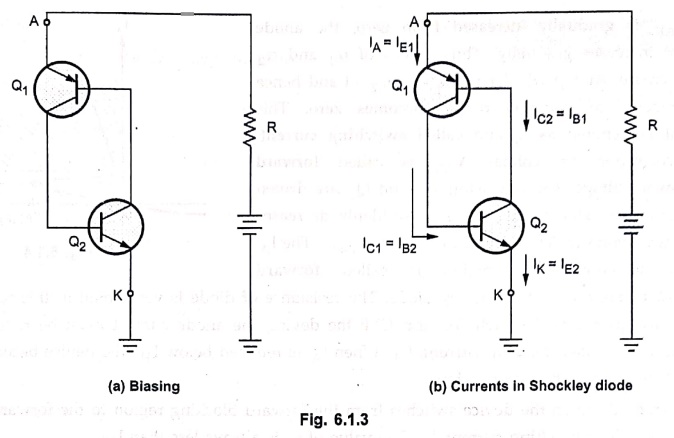
Consider the biasing provided to the Shockley diode as shown in the Fig. 6.1.3
(a). The various currents, due to the biasing arrangement are shown in the Fig.
6.1.3 (b).
•
As per the requirement, junctions J1, J3 are forward
biased while the junction J3 is reverse biased. So both the
transistors are operating in linear region.
•
Expression for IA: For
low forward biased voltages let us obtain the expression for IA using
standard transistor relations. Considering the reverse leakage currents ICBO1
and ICBO2 through reverse biased collector base junctions, we can
write,
IB1 = IE1‒IC1
‒ICB01
But
IC1=
α1IE1
IB1
= IE1 ‒ α1IE1 ‒ ICB01 = (1‒α1)IE1‒ICB01
Now
IE1
= IA = Anode current
IB1 = (1‒α1)IA ‒ ICB01
For
transistor Q2,
IC2 = α2IE2
+ICBO2
But
IE2
= IK = Cathode current
IC2
= α2IK + ICBO2
But
IC2
= IB1
………….. Connected together
(1‒α1)IA
‒ ICB01 = α2IK +ICBO2
But
IA
= IK
……………Current entering and leaving
(1‒α1)IA ‒ ICB01
= α2IA +ICBO2
IA
[1‒ α1‒ α2] = ICB01 + ICBO2
IA = [ ICB01 + ICBO2 ] / [1‒(α1+α2)]
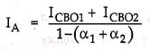
where
α1 and α2 are the d.c. current gains for the transistors,
the values of which are very small. The reverase currents ICBO1 and
ICBO2 are also small. Hence for small bias levels, the diode is said
to be OFF which is its forward blocking region.
Characteristics of Shockley Diode
•
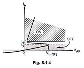
We have seen that when the Shockley diode is forward biased, it is essentially
OFF and acts as an open switch. This region for small forward bias level for
which the diode remains OFF is called forward blocking region. The device has
very high forward resistance, ideally ∞. The region continues from VAK
= 0 to a specific voltage called forward breakover voltage VBR (F).
This is shown in Fig. 6.1.4.
•
As VAK is gradually increased from zero, the anode current increases
gradually. Thus values of α1 and α2 also increase. At a
particular point, α1+a2 =1 and hence denominator of
equation of IA becomes zero. This current is denoted as IS
and called switching current. The corresponding voltage VAK is
called forward breakover voltage. The transistors Q1 and Q2
are driven into saturation. Due to this, the VAK suddenly decreases
to the low value which is equal to VBE +VCE(sat). The IA
further increases. This region is called forward conduction region of the
Shockley diode. The resistance of diode is very small in this region and the
device acts as a closed switch. To turn OFF the device, the anode current must
be reduced below a specific value, called holding current, IH. When
IA is reduced below IH, the device becomes OFF and enters
into forward blocking region.
•
The current at which the device switches from the forward blocking region to
the forward conduction region, is called switching current, IS. The
value of IS is always less than IH.
Ex. 6.1.1: A certain Shockley diode is in its
forward blocking region. The d.c. a values for the two transistors are α1
= 0.3 and α2 = 0.4. The leakage currents for both are 125 nA.
Calculate the anode current. If the anode to cathode voltage is 15 V, calculate
forward resistance of the diode.
Solution:
α1= 0.3, α2 = 0.4, ICBO1 = ICBO2 = 125 nA, VAK = 15 V
IA
= [ ICB01 + ICBO2 ]
/ [ 1‒(α1+α2) ]
=
[125×2×10‒9] / [1‒(0.3+0.4)]
=
0.833 μ Α
and
Rf
= VAK / IA
=
15 / 0.833×10‒6
=
18 MΩ
Thus
the forward resistance of shockley diode in the forward blocking region is very
very high and it acts as an open switch.
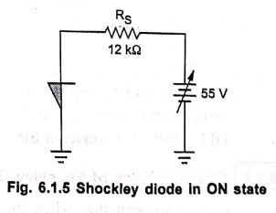
Ex. 6.1.2: Find the value of anode current
for the device shown in the Fig. 6.1.5 which is ON. VBR(F) = 40 V.
Assume VBE = 0.71V and VCE(sat) = 0.15 V for the internal
transistor. Also find the forward resistance of the diode.
Solution:
VAK
= VBE + VCE(sat)
=
0.71+ 0.15 = 0.86 V
... Device ON
VRS
= VBIAS ‒VAK
= 55‒0.86 = 54.14 V
IA
= VRS / RS
=
54.14 / 12×103
=
4.511 mA
Rf
= VAK / ΙΑ
=
0.86 / 4.511×10‒3
=
190.64 Ω
So
Rf in ON state is very low.
Application
•
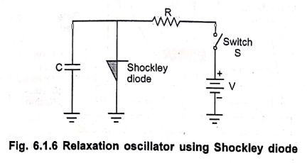
Fig. 6.1.6 shows the use of the Shockley diode in a relaxation oscillator.
•
When the switch S is closed, the capacitor starts charging through R. When the
voltage across capacitor reaches to breakover voltage of diode, the diode
becomes ON and acts as closed switch. The capacitor discharges rapidly through
the diode. When the device current becomes less than the holding current, it
turns OFF and the capacitor starts its charging again.
•
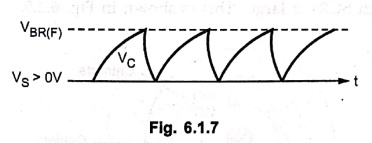
The waveform of the voltage across the capacitor C is shown in Fig. 6.1.7.
•
The capacitor will not discharge completely but a voltage level corresponding
to switching current denoted as VS which is slightly more than 0 V.
Review
Questions
1. Explain the construction and working of Shockley diode.
2. Draw and explain the characteristics of Shockley diode
stating its applications.
Electron Devices: Chapter 6: Thyristors UJT and Optoelectronic Devices : Tag: electronics : construction, Working Operation, Symbol, Characteristics, Equivalent Circuit, Application, Example Solved Problems - Shockley Diode
Electron Devices: Chapter 6: Thyristors UJT and Optoelectronic Devices
Under Subject

Electron Devices
EC25C01 2nd Semester ECE Dept | 2025 Regulation | 2nd Semester 2025 Regulation
Related Subjects

English Essentials II
EN25C02 2nd Semester | 2025 Regulation | 2nd Semester 2025 Regulation

Tamils and Technology தமிழர்களும் தொழில்நுட்பமும்
UC25H02 2nd Semester | 2025 Regulation | 2nd Semester 2025 Regulation

Linear Algebra
MA25C02 2nd Semester | 2025 Regulation
Electron Devices
EC25C01 2nd Semester ECE Dept | 2025 Regulation | 2nd Semester 2025 Regulation

Data Structures using CPlusPlus
CS25C05 2nd Semester ECE Dept | 2025 Regulation | 2nd Semester 2025 Regulation

Circuits and Network Analysis
EC25C02 2nd Semester ECE Dept | 2025 Regulation | 2nd Semester 2025 Regulation

Re-Engineering for Innovation
ME25C05 2nd Semester | 2025 Regulation | 2nd Semester 2025 Regulation

Engineering Drawing - Laboratory
ME25C01 2nd Semester | 2025 Regulation | 2nd Semester 2025 Regulation

Data Structures using CPlusPlus - Laboratory
CS25C05 2nd Semester ECE Dept | 2025 Regulation | 2nd Semester 2025 Regulation

Devices and Circuits Laboratory
EC25C03 2nd Semester ECE Dept | 2025 Regulation | 2nd Semester 2025 Regulation