Electron Devices: Chapter 6: Thyristors UJT and Optoelectronic Devices
Photovoltaic Cell or Solar Cell
Construction, Working Principle, Symbol, Characteristics, Applications

Questions: 1. Explain the construction, symbol and characteristics of photovoltaic cell. 2. List the applications of photovoltaic cell. 3. Write a note on solar cell.
Photovoltaic
Cell or Solar Cell
•
The solar cell is nothing but a photovoltaic cell which works on the principle
of photovoltaic effect. The solar cell generates voltage proportional to the
light incident on it.
•
A solid state device which converts the light energy into an electrical energy
based on photovoltaic effect is called a solar cell.
1. Construction and Working
•
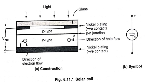
Fig. 6.11.1 (a) shows the construction of a solar cell while the Fig. 6.11.1
(b) shows the symbol of a solar cell.
•
The surface layer of p‒type material is extremely thin so that light can
penetrate to the junction.
•
The nickel plated ring around p‒type is the positive output terminal. The
nickel plated ring around n‒type material acts as the negative output terminal.
•
When the light strikes the cell, the photon light energy is absorbed by the
semiconductor material and number of electron‒hole pairs are generated. This
happens on both the sides of the junction.
•
The holes are directed towards the p‒region while the electrons are directed
towards the n‒region due to the electric field present. Due to this movement
the minority current is set up across the junction due to which the voltage is
developed across the p and n regions. This voltage is taken out as the output
voltage.
•
The selenium and silicon are most widely used materials for the solar cells.
The gallium arsenide, indium arsenide nd cadmium sulphide are also used for the
solar cells.
•
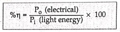
The efficiency of solar cell is the ratio of electrical power output to the
power input by the light source. It is typically between 15 to 40 %.
%η = [ P0(electrical) / Pi(light
energy) ] × 100
2. Characteristics
•
When light strikes the cell, certain portion of it is absorbed within the
semiconductor material. This means that the energy of the absorbed light is
transferred to the semiconductor.
•
This photon light energy collides with a valence electron and imparts to it
sufficient energy to leave the parent atom. This results in the generation of
free electrons and holes. This phenomenon will occur on each side of the
junction.
•
In the p‒type material, the newly generated electrons are minority carriers and
will move rather freely across the junction as explained for the basic p‒n
junction.
•
A similar discussion is true for the holes generated in the n‒type material.
•
The result is an increase in the minority carrier flow which is opposite in
direction to the conventional forward current of a p‒n junction.
•
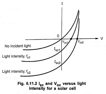
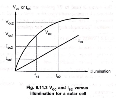
Fig. 6.11.2 shows the characteristics of solar cell.
• At vertical axis, V = 0 and it is short circuit condition. The short circuit current is represented by notation ISC.
•
Under open circuit condition I = 0 and photovoltaic voltage Voc will result.
3. Materials
•
Selenium and silicon are the most widely used materials for solar cells,
although gallium arsenide, indium arsenide, and cadmium sulphide, among others,
are also used.
•
However, silicon has a higher conversion efficiency and greater stability and
is less subjected to fatigue. It also has excellent temperature
characteristics. That is, it withstand can extreme high high or low
temperatures without a significant drop‒off in efficiency.
4. Applications
•
The various applications of solar cell are,
1.
Satellites and space vehicles.
2.
Automated street lights.
3.
Power supply to calculators.
4.
Emergency lights.
5.
For charging the batteries.
6.
Solar panels for domestic purposes, water pumps etc.
• In practice to get desired output power, the solar cells are connected in series and such groups are connected in parallel. This is called array of solar cell and shown in Fig. 6.11.4.
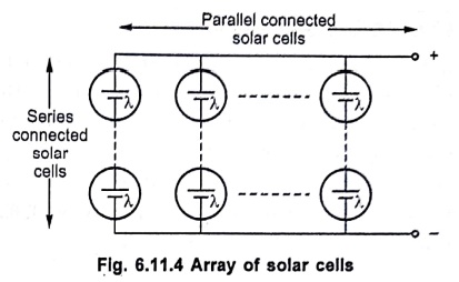
• The series solar cells provide necessary output voltage while parallel groups provide necessary output current.
Review
Questions
1. Explain the construction, symbol and characteristics of
photovoltaic cell.
2. List the applications of photovoltaic cell.
3. Write a note on solar cell.
Electron Devices: Chapter 6: Thyristors UJT and Optoelectronic Devices : Tag: electronics : Construction, Working Principle, Symbol, Characteristics, Applications - Photovoltaic Cell or Solar Cell
Electron Devices: Chapter 6: Thyristors UJT and Optoelectronic Devices
Under Subject

Electron Devices
EC25C01 2nd Semester ECE Dept | 2025 Regulation | 2nd Semester 2025 Regulation
Related Subjects

English Essentials II
EN25C02 2nd Semester | 2025 Regulation | 2nd Semester 2025 Regulation

Tamils and Technology தமிழர்களும் தொழில்நுட்பமும்
UC25H02 2nd Semester | 2025 Regulation | 2nd Semester 2025 Regulation

Linear Algebra
MA25C02 2nd Semester | 2025 Regulation
Electron Devices
EC25C01 2nd Semester ECE Dept | 2025 Regulation | 2nd Semester 2025 Regulation

Data Structures using CPlusPlus
CS25C05 2nd Semester ECE Dept | 2025 Regulation | 2nd Semester 2025 Regulation

Circuits and Network Analysis
EC25C02 2nd Semester ECE Dept | 2025 Regulation | 2nd Semester 2025 Regulation

Re-Engineering for Innovation
ME25C05 2nd Semester | 2025 Regulation | 2nd Semester 2025 Regulation

Engineering Drawing - Laboratory
ME25C01 2nd Semester | 2025 Regulation | 2nd Semester 2025 Regulation

Data Structures using CPlusPlus - Laboratory
CS25C05 2nd Semester ECE Dept | 2025 Regulation | 2nd Semester 2025 Regulation

Devices and Circuits Laboratory
EC25C03 2nd Semester ECE Dept | 2025 Regulation | 2nd Semester 2025 Regulation