Electron Devices: Chapter 6: Thyristors UJT and Optoelectronic Devices
Power MOSFET
Features, Structure, Working Principle, Characteristics

Questions: 1. State the features of power MOSFET. 2. Draw and explain the DMOS structure. 3. Draw and explain the VMOS structure. 4. Draw and explain the characteristics of power MOSFET. 5. Write a note on safe operating area of power MOSFET. 6. Write a short note on power MOSFET. 7. What is the name implies VMOS?
Power
MOSFET
•
The operation of power MOSFET is same as that of conventional MOSFET but the
power handling capacity of conventional MOSFET is less than 1 W.
•
New designs and recent manufacturing techniques have been developed to produce
more complicated three dimensional gate structure which is used in power
MOSFETs.
•
The features of power MOSFET are,
1.
The power handling capacity is more than 100 W.
2.
The current handling capacity is in the ampere why range.
3.
The drain to source blocking voltage may be more than 100 V.
4.
Large forward transconductance.
5.
The control signal is applied to gate whose input impedance is very high hence
large currents can be switched with very small control currents.
•
The two types of structures used in are, i) DMOS (Double Diffused) ii) VMOS
(Vertical Channel).
1. DMOS Structure
•
It is an asymmetric power MOSFET designed for low ON resistance and high
blocking voltage. This device has a shorter channel between drain and source
than the conventional MOSFET.
•
The device uses double diffusion process.
•
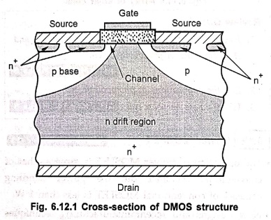
Fig. 6.12.1 shows the cross‒sectional view of DMOS structure.
•
The p base region and n+ source region are diffused through a common
window existing at the edge of the gate.
•
The P base is diffused deeper than n+ source. The source channel
length is decided by the difference between diffusion distances of p base and
the n+ source, which is very short.
•
Electrons enter the source terminal and laterally flow through the layer under
the gate to the n drift region.
•
Then the electrons flow vertically to the drain terminal through the n drift
region.
•
The drift region is moderately doped so that drain breakdown voltage is high
while drift region is very thin which keeps drain resistance to very small
value.
•
This device is used in RF power amplifiers in base stations of wireless
communication systems and in numerous UHF and L‒band power amplifiers in
broadcast, communication and radar systems.
2. VMOS Structure
•
This is vertical structure with V shaped groove creating shorter and wider
channel. This helps to increase power handling and current handling capacity of
the device. Because of V shaped structure it is known as VMOS.
•
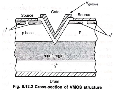
Fig. 6.12.2 shows the construction of VMOS structure.
•
It consists of a double diffused n+/p layer, which is cut by a V
shaped groove.
•
The V shaped groove is easily fabricated by anisotropically etching a silicon
surface using a concentrated KOH solution.
•
The V shaped groove is then coated with a gate oxide (SiO2), followed
by the gate electrode.
•
As the V shaped groove cuts through the double diffused layer, it creats two
vertical MOSFETs, one on each side of the groove.
• The combination of V shaped groove with the double diffused layers results in a short gate length which is determined by the thickness of the p type layer.
•
The vertical structure allows the use of a low doped drain region, which
results in a high blocking voltage.
•
The channel is induced vertically along both sides of the V shaped groove
between the source and the drain connection.
3. Characteristics of Power MOSFET
•
The resistance when power MOSFET is ON, is an important parameter.
•
The ON resistance is given by,
RON = RD + RS
+RCH
where,
RD
= Drain resistance,
RS
= Source resistance a
RCH
= Channel resistance
•
In power MOSFET all the three resistance values are significant though in
conventional MOSFET, RD and RS are very small.
•
As temperature increases, threshold voltage changes which may increase current.
•
As current increases, temperature increases due to which mobility decreases.
•
RCH is inversely proportional to the mobility hence RCH
increases which limits the current in power MOSFET.
•
The threshold voltage VGS(th) is defined as the minimum gate
electrode bias required to strongly invert the surface under the poly and form
a conducting channel between the source and the drain regions.
•
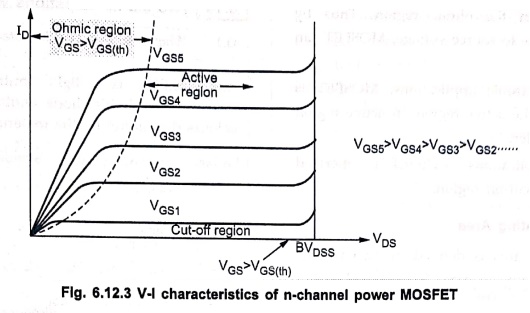
Fig. 6.12.3 shows the V‒I characteristics of n channel power MOSFET.
•
The drain current iD is plotted with respect to drain to source
voltage VDS. These characteristics are plotted for various values of
gate source voltage (VGS).
•
In Fig. 6.12.3 observe that there are three regions in the characteristics:
Ohmic region, active region and cutoff region.
•
In the cutoff region, the drain current is negligible and the MOSFET is said to
be in 'OFF' state. The MOSFET is driven in cutoff region by applying VGS
< VGS (th). Here VGS(th) is the threshold gate source
voltage. When gate to source voltage is less than threshold gate source voltage,
MOSFET is off, i.e. in cutoff region.
•
The MOSFET is driven in cutoff region by applying VGS < VGS(th).
Here VGS(th) is the threshold gate source voltage. When gate to
source voltage is less than threshold gate source voltage, MOSFET is off, i.e.
in cutoff region. The MOSFET is driven into ohmic region when VGS
>> VGS (th). In the ohmic region, the MOSFET conducts heavily.
Hence it is said to be 'on' in the ohmic region. Thus by applying heavy gate to
source voltage, MOSFET can be turned on.
•
In the power electronic applications, MOSFET is never operated in the active
region. In active region it acts as an amplifier.
•
For switching applications, MOSFET is operated only in ohmic and cut‒off
regions.
4. Safe Operating Area
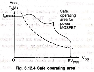
The
safe operating area is defined by two factors, the maximum drain current ID
max and rated breakdown voltage BVDSS.
•
The maximum power that power MOSFET can deliver is given by,
Pmax = ID VSS
•
Fig. 6.12.4 shows the safe operating area for power MOSFET.
Review
Questions
1. State the features of power MOSFET.
2. Draw and explain the DMOS structure.
3. Draw and explain the VMOS structure.
4. Draw and explain the characteristics of power MOSFET.
5. Write a note on safe operating area of power MOSFET.
6. Write a short note on power MOSFET.
7. What is the name implies VMOS?
Electron Devices: Chapter 6: Thyristors UJT and Optoelectronic Devices : Tag: electronics : Features, Structure, Working Principle, Characteristics - Power MOSFET
Electron Devices: Chapter 6: Thyristors UJT and Optoelectronic Devices
Under Subject

Electron Devices
EC25C01 2nd Semester ECE Dept | 2025 Regulation | 2nd Semester 2025 Regulation
Related Subjects

English Essentials II
EN25C02 2nd Semester | 2025 Regulation | 2nd Semester 2025 Regulation

Tamils and Technology தமிழர்களும் தொழில்நுட்பமும்
UC25H02 2nd Semester | 2025 Regulation | 2nd Semester 2025 Regulation

Linear Algebra
MA25C02 2nd Semester | 2025 Regulation
Electron Devices
EC25C01 2nd Semester ECE Dept | 2025 Regulation | 2nd Semester 2025 Regulation

Data Structures using CPlusPlus
CS25C05 2nd Semester ECE Dept | 2025 Regulation | 2nd Semester 2025 Regulation

Circuits and Network Analysis
EC25C02 2nd Semester ECE Dept | 2025 Regulation | 2nd Semester 2025 Regulation

Re-Engineering for Innovation
ME25C05 2nd Semester | 2025 Regulation | 2nd Semester 2025 Regulation

Engineering Drawing - Laboratory
ME25C01 2nd Semester | 2025 Regulation | 2nd Semester 2025 Regulation

Data Structures using CPlusPlus - Laboratory
CS25C05 2nd Semester ECE Dept | 2025 Regulation | 2nd Semester 2025 Regulation

Devices and Circuits Laboratory
EC25C03 2nd Semester ECE Dept | 2025 Regulation | 2nd Semester 2025 Regulation