Electron Devices: Chapter 6: Thyristors UJT and Optoelectronic Devices
Thyristors UJT and Optoelectronic Devices: Two Marks Important Questions and Answers
Electron Devices
Electron Devices: Chapter 6: Thyristors UJT and Optoelectronic Devices: Anna University Part A Two Marks Important Questions and Answers
Electron
Devices
Chapter 6: Thyristors UJT
and Optoelectronic Devices
Two Marks
Questions with Answers
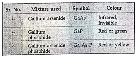
1. What is LED? Which
material is used for LED ?
LED is a light emitting diode. When forward
biased this diode emits light of different colours depending on the material
used.
2. List any four
applications of light emitting diode.
1.
All kinds of displays used in watches and calculators.
2.
In the optical devices such as opto‒couplers.
3.
As on‒off indicator in various electronic circuits.
4.
In remote controls and burgler alarms.
3. What are the advantages
of LCD ?
1.
Less power consumption.
2.
Low cost.
3.
Uniform brightness with good contrast.
4.
Low operating voltage and current.
4. What are the
disadvantages of LCD.
1.
Poor reliability.
2.
Limited temperature range.
3.
Poor visibility in low ambient temperature.
4.
Slow speed.
5.
Requires an a.c. drive.
5. State the three main
categories of LCD.
1.
Smectic 2. Nematic 3. Cholesteric.
6. What is SCR? Explain its
construction in brief.
SCR
is a silicon controlled rectifier.
The
SCR is a four layer p‒n‒p‒n device where P and n layers are alternately
arranged. The outer layers are heavily doped. There are three p‒n junctions
called J1, J2 and J3. The outer p layer is
called anode while outer n layer is called cathode. Middle p layer is called
gate. The three terminals are taken out respectively from these three layers.
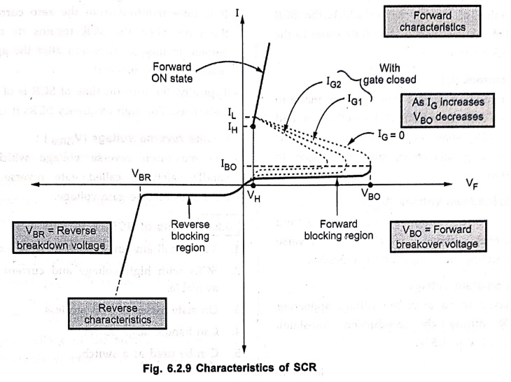
7. Draw the characteristics
of SCR.
8. State any four
specifications of SCR.
1.
Forward Breakover Voltage (VBO): It is the
voltage above which the SCR enters the conduction region ('ON' state). The
forward breakdown voltage is dependent on the gate bias.
2.
Holding Current (IH): It is that value of
current below which the SCR switches from the conduction state (ON state) to
the forward blocking state.
3.
Latching Current (IL): This is the minimum
current flowing from anode to cathode when SCR goes from OFF to ON state and
remains in ON state even after gate bias is removed. It is greater than, but
very close to holding current.
4.
Reverse Breakdown Voltage (VBR): It is the
voltage (Anode‒negative cathode‒positive) above which the reverse breakdown
occurs, breaking J1 and J3 junctions. When the SCR is
reversed biased, the thickness of the J2 depletion layer during the
forward bias condition is greater than the total thickness of the two depletion
layers at J1 and J3. Therefore, the forward breakover
voltage VBO is greater than the reverse breakover voltage VBR.
9. State the applications
of SCR.
1.
Controlled rectifiers.
2.
A.C. voltage stabilizers.
3.
D.C. to D.C. converters called choppers.
4.
D.C. to A.C. converters called inverters.
5.
Dimmerstats to control light intensity.
6.
For speed control schemes of d.c. and a.c. motors called drives.
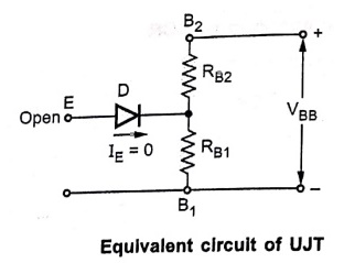
10. Draw the equivalent
circult of UJT.
11. What Is Interbase
resistance of UJT ?
When
the emitter diode is not conducting then the resistance between the two bases B1
and B2 is called interbase resistance denoted as RBB.
RBB = RB1+RB2
Its
value ranges between 4 kΩ and 12 kΩ.
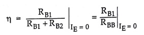
12. Define intrinsic stand
off ratio for UJT.
For
UJT intrinsic stand off ratio is defined as
13. Draw the
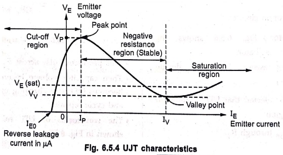
characteristics of UJT.
14. State the applications
of UJT.
1.
Triggering of other devices like SCR.
2.
In a sawtooth waveform generator.
3.
In a relaxation oscillator.
4.
In timing circuits.
5.
In automobile ignition circuits.
15. Draw the diac
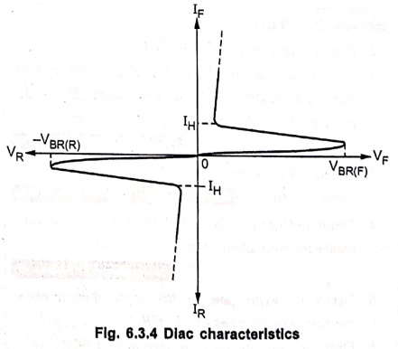
characteristics.
16. State the applications
of diac.
1.
Triggering of triac
2.
Motor speed control
3.
Temperature control
4.
Light dimming circuit
5.
In air conditioning and other domestic applications.
17. Draw the
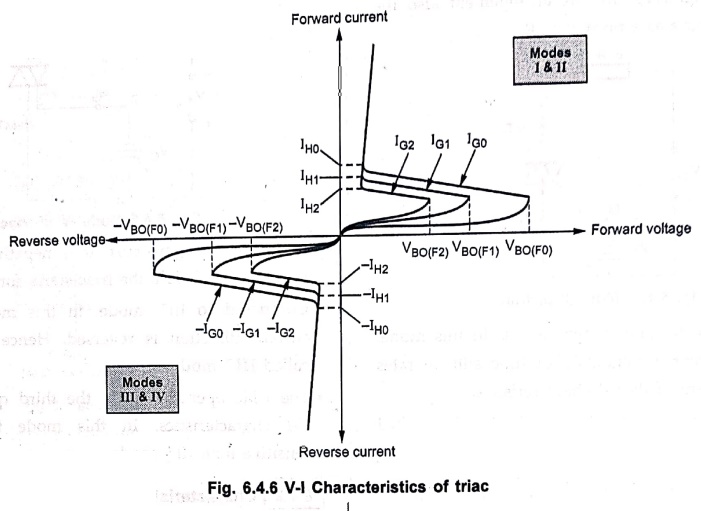
characteristics of triac.
18. State the applications
of triac.
1.
Static d.c. switching of applications.
2.
In a three position static switch.
3.
A.C. power flashers.
4.
Heater or temperature controllers.
5.
As a triggering device for SCRS.
6.
Light dimmer circuits.
19. Compare SCR and triac.
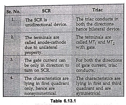
SCR
1.
The SCR is unidirectional device.
2.
The terminals are called anode‒cathode due to unilateral property.
3.
The gate current can be only in direction to turn on SCR
4.
The characteristics are lying in first quadrant only, hence are nonsymmetrical.
Triac
1.
The triac conducts in both the directions hence bilateral device.
2.
The terminals are called MT1 and MT2 with gate.
3.
For both the directions of gate current, triac conducts.
4.
The characteristics are lying in first and third quadrant and are symmetrical.
20. State the applications
of phototransistor.
1.
Punch card readers
2.
Computer logic circuitry
3.
Lighting control
4.
Level indicators
5.
Relays.
21. What is photoconductive
cell?
The
photoconductive cell is semiconductor device whose resistance varies inversely
with the intensity of light that falls upon its photosensitive material. These
devices are also called photoresistive cells or photoresistors, since the
change in conductivity appears as a change in resistance.
22. State the applications
of photoconductive cell.
1.
Smoke detecters
2.
Burglar alarm
3.
Outdoor lighting control.
4.
Photographic instruments
5.
Punch card readers.
23. What is photovoltaic
cell ?
A
solid state device which converts light energy into an electrical energy based
on photovoltaic effect is called photovoltaic cell or solar cell. It generates
voltage proportional to the light incident on it.
24. State the applications
of photovoltaic cell.
1.
Satellites and space vehicles.
2.
Automated street lights.
3.
Power supply to calculators.
4.
Emergency lights.
5.
For charging the batteries.
6.
Solar panels for domestic purposes, water pumps etc.
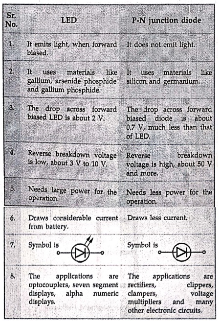
25. Compare LED and LCD.
26. Draw the basic
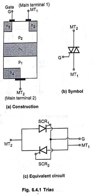
structure of TRIAC and its symbol.
27. Write down the significance
of opto coupler.
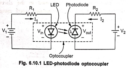
A
package which is a combination of light source like LED and a light detector as
photodiode or phototransistor is called optocoupler. In optocoupler if input
voltage changes then light emitted by light source changes. This changes the
characteristics of a light detector hence output voltage changes. Thus output
voltage is optically coupled with the input voltage, though electrically
isolated. Thus the device couples input to output circuit optically, providing
electrical isolation.
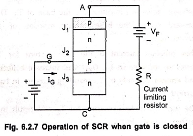
28. Draw the two transistor
equivalent circuit of an SCR.
29. A solar cell is a pn
junction device with no voltage directly applied across the junction". If
it is so, how does a solar cell deliver power to a load ?
A
solar cell is a photovoltaic cell which converts the light energy incident on
it into an electrical energy based on photovoltaic effect. This electrical
energy is in the form of internally generated voltage across the junction due
to the movement of minority charge carriers across the junction due to light
energy. This voltage delivers power to the load hence no external voltage is
required to be applied across the junction.
30. Draw the circuit
diagram of opto coupler.
31. What is meant by
regenerative action of SCR?
•
Consider that the voltage is applied between gate and cathode when the SCR is
in forward blocking state.
•
The gate is made positive with respect to the cathode.
•
The electrons from n‒type cathode which are majority in number, cross the
junction J3 to reach to positive of battery.
•
While holes from p type move towards the negative of battery, this constitutes
the gate current.
•
This current increases the anode current as some of the electrons cross
junction J2. As anode current increases, more electrons cross the
junction J2 and the anode current further increases.
•
This action is called regenerative action in SCR. Due to this within short time
junction J2 breaks and SCR conducts heavily,
32. Glue the symbol,
structure and equivalent clrcult of DIAC ?
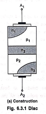
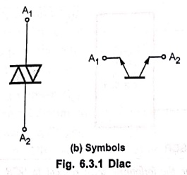
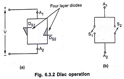
33. What is the effect of
temperature on solar cell?
The
efficiency of solar cell decreases as the temperature increases. The effect of
temperature on solar cell is known as temperature coefficient. For silicon solar
cells, the efficiency decreases by 0.45 % for every degree rise in temperature.
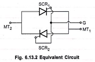
34. Draw the symbol and equivalent circuit of TRIAC ?
The
equivalent circuit is shown in the Fig. 6.13.2.
35. Define quantum efficiency
in an LED.
The
fraction of the electrons that are injected into the depletion (active) region
which results in photons getting produced is known as internal quantum
efficiency in LED. It is defined by the number of photons generated from a
given active region divided by the number of injected electrons.
Electron Devices: Chapter 6: Thyristors UJT and Optoelectronic Devices : Tag: electronics : Electron Devices - Thyristors UJT and Optoelectronic Devices: Two Marks Important Questions and Answers
Electron Devices: Chapter 6: Thyristors UJT and Optoelectronic Devices
Under Subject

Electron Devices
EC25C01 2nd Semester ECE Dept | 2025 Regulation | 2nd Semester 2025 Regulation
Related Subjects

English Essentials II
EN25C02 2nd Semester | 2025 Regulation | 2nd Semester 2025 Regulation

Tamils and Technology தமிழர்களும் தொழில்நுட்பமும்
UC25H02 2nd Semester | 2025 Regulation | 2nd Semester 2025 Regulation

Linear Algebra
MA25C02 2nd Semester | 2025 Regulation
Electron Devices
EC25C01 2nd Semester ECE Dept | 2025 Regulation | 2nd Semester 2025 Regulation

Data Structures using CPlusPlus
CS25C05 2nd Semester ECE Dept | 2025 Regulation | 2nd Semester 2025 Regulation

Circuits and Network Analysis
EC25C02 2nd Semester ECE Dept | 2025 Regulation | 2nd Semester 2025 Regulation

Re-Engineering for Innovation
ME25C05 2nd Semester | 2025 Regulation | 2nd Semester 2025 Regulation

Engineering Drawing - Laboratory
ME25C01 2nd Semester | 2025 Regulation | 2nd Semester 2025 Regulation

Data Structures using CPlusPlus - Laboratory
CS25C05 2nd Semester ECE Dept | 2025 Regulation | 2nd Semester 2025 Regulation

Devices and Circuits Laboratory
EC25C03 2nd Semester ECE Dept | 2025 Regulation | 2nd Semester 2025 Regulation