Electron Devices: Chapter 6: Thyristors UJT and Optoelectronic Devices
Silicon Controlled Rectifier (SCR)
Types of Construction, Working Principle, Two Transistor Model, Characteristics, Symbol, Equivalent Circuit, Parameters, Merits, Demerits, Applications, Crowbar Circuit

Questions: 1. Explain the construction of SCR. 2. Enumerate the structure of a SCR, with a two transistor model derive an expression for anode current (IA) Also indicate its V‒I characteristics. 3. Explain the working principle of SCR and its V‒I characteristics. 4. Draw and explain the operation of SCR using two transistor equivalent circuit. 5. Derive the expression for the anode current from the two transistor model of SCR. 6. Draw and explain the characteristics of SCR. 7. Define the following with respect to SCR: i. Forward breakover voltage ii. Holding current iii. Latching current iv. Reverse breakdown voltage. 8. State the various specifications of SCR. 9. State the merits of SCR. 10. State the demerits of SCR. 11. State the various applications of SCR. 12. Explain the operation, characteristics and applications of SCR.
Silicon
Controlled Rectifier (SCR)
•
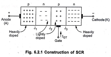
The SCR is a four layer p‒n‒p‒n device where P and n layers are alternately
arranged. The outer layers are heavily doped while inner layers are lightly
doped.
•
There are three p‒n junctions called J1, J2 and J3.
•
The outer p layer is called anode while outer n layer is called cathode. Middle
p layer is called gate.
•
The three terminals are taken out respectively from these three layers, as
shown in Fig. 6.2.1.
•
Fig. 6.2.1 Construction of SCR
•
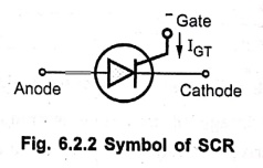
Anode must be positive with respect to cathode to forward bias the SCR.
•
But this is not sufficient criterion to turn SCR ON. To make it ON, a current
is to be passed through the gate terminal denoted as IGT. Thus it is
a current operated device.
•
The IGT is the gate trigger current required to make the SCR ON.
•
The basic material used for the SCR fabrication is silicon.
1. Types of Construction
•
Three types of constructions are used to manufacture SCR,
1)
Planar type
2)
Mesa type
3)
Press pack type.
1. Planar type:
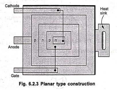
This
construction is used for low current SCRs. In this type, all the p‒n junctions
come to the same surface on the cathode side. This is shown in Fig. 6.2.3. All
the junctions are diffused in this type of construction.
•
The disadvantage of this type is more silicon per ampere current is required.
The advantage is that the mass production is possible and large number of SCRs
can be manufactured with uniform characteristics.
2. Mesa type:
•
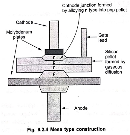
In this construction, the junction J2 is diffused while the outer
layers are alloyed to it. This is shown in Fig. 6.2.4.
•
To handle the large currents, the molybdenum or tungsten plates are braced to p‒n‒p‒n
silicon pellet. This provides the additional mechanical strength.
• In this construction, area around the gate is small hence this construction is not suitable for high di/dt ratings.
3. Press pack type:
•
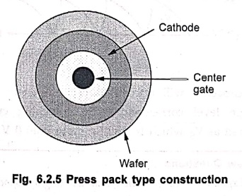
The construction is used for high power and center gate SCRS. A silicon wafer
is used to make such a high power SCR.
•
The entire circular area around the gate takes part in the initial conduction
hence di/dt capability of such SCRS is large. This is shown in Fig. 6.2.5.
•
This type of construction provides double sided cooling arrangement which is
necessary for high power SCRs.
2. Working Principle
•
The operation of SCR is divided into two categories,
i)
When Gate is open and
ii)
When Gate is closed.
1. When gate is open :
•
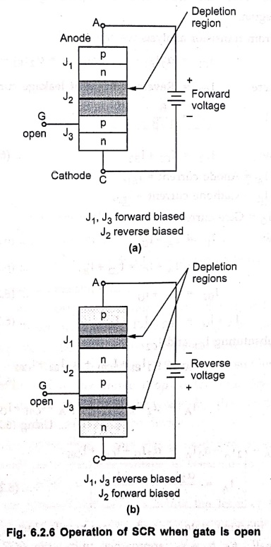
Consider that the anode is positive with respect to cathode and gate is open.
•
The junctions J1 and J3 are forward biased and junction J2
is reverse biased. There is depletion region around J2 and only
leakage current flows which is negligibly small.
•
Practically the SCR is said to be OFF. This is called forward blocking state of
SCR and voltage applied to anode and cathode with anode positive is called
forward voltage. This is shown in Fig. 6.2.6 (a).
•
With gate open, if cathode is made positive with respect to anode, the
junctions J1, J3 become reverse biased and J2
forward biased. Still the current flowing is leakage current, which can be
neglected as it is very small.
• The voltage applied to make cathode positive is called reverse voltage and SCR is said to be in reverse blocking state. This is shown in Fig. 6.2.6 (b).
•
In forward blocking state, if the forward voltage is increased and made
suficiently large, the reverse biased junction J2 breaks down and
SCR conducts heavily. This voltage is called forward breakover voltage VBO
of SCR. In such condition, SCR is said to be ON or triggered.
2. When gate is closed :
•
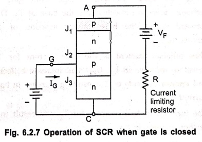
Consider that the voltage is applied between gate and cathode when the SCR is
in forward blocking state.
•
The gate is made positive with respect to the cathode.
•
The electrons from n‒type cathode which are majority in number, cross the
junction J3 to reach to positive of battery.
•
While holes from p type move towards the negative of battery, this constitutes
the gate current.
•
This current increases the anode current as some of the electrons cross
junction J2. As anode current increases, more electrons cross the
junction J2 and the anode current further increases.
•
Due to regenerative action, within short time, the junction J2
breaks and SCR conducts heavily. The connections are shown in Fig. 6.2.7. The
resistance R is required to limit the current.
• Once the SCR conducts, the gate loses its control.
3. Two Transistor Model
•
The two transistor model of SCR is shown in Fig. 6.2.8.
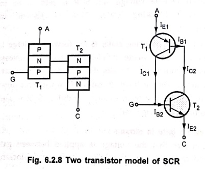
Fig. 6.2.8 Two transistor model of SCR
•
The left half is a pnp transistor and right half is npn transistor.
•
The collector current of T1 becomes base current of T2
and collector current of T2 becomes base current of T1.
•
Consider a positive voltage on the anode with respect to the cathode and gate
current is zero.
•
As gate current is zero, base current of T2, IB2 is zero
and IC2 is approximately ICO.
•
The base current of T1, IB1 = IC2 = ICO,
is too small to turn T1 ON. Both transistors are therefore in the
"OFF" state, resulting in a high impedance between the collector and
emitter of each transistor.
•
The anode current is then just the sum of the leakage currents of the two
transistors, ICO1 + ICO2.
•
When we apply positive voltage from gate to cathode, holes are injected into
the base of T2. This forward biases the base emitter junction of T2
increasing IC2.
•
This collector current is the base current for T1, therefore
increase in IC2 (IB1) will increase collector and emitter
currents of T1, resulting increase in base current of T2.
•
The increase in base current for T2 will result in a further
increase in IC2.
•
The net result is a regenerative increase in the collector current of each
transistor. This regenerative process is continuous until both transistors are
driven into saturation making all junctions forward biased.
•
This results in large anode current which is limited only by the external
circuit resistance and voltage.
•
Let IC1 and IC2 are collector currents, IE1
and IE2 are emitter currents while IB1 and IB2
are base currents of transistors T1 and T2.
•
Let both the transistors are operating in active region.
•
From transistor analysis we can write,
IC1 = α1IE1
+IC01 and IC2 = α21E2 + ICO2
where
ICO = Reverse current or
leakage current
and
α = β /
1+β
Now
IE2 = IC2 + IB2
…… (6.2.1)
IA
= Anode current = IEI
IK
= Cathode current = IE2,
IG
= Gate current
Now
IK
= IA + IG …… (6.2.2)
IE2
= IA+IG = IC2+IB2 …… (6.2.3)
But
IB2 = IC1 + IG …… (6.2.4)
IA+IG
= IC2 + IC1 + IG …… (6.2.5)
Substituting
IC1 and IC2,
IA = α1IE1 + IC01
+ α2IE2 +IC02
…… (6.2.6)
ΙΑ
= α2 (IA + IG) + α1IA +IC01
+IC02
………Using (6.2.3)
ΙΑ ‒ α2IA ‒ α1IA
= α2IG +IC01 +IC02
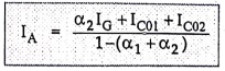
IA = [ a2IG +
IC01 + IC02 ] / [ 1‒(α1+α2) ]
…… (6.2.7)
• In blocking state α1 and α2 are small. Thus IA is small. As α1+α2 approaches unity, the SCR is ready to enter into conduction. Then due to positive gate current, the regenerative action takes place and SCR conducts.
4. Characteristics of SCR
•
Fig. 6.2.9 shows the characteristics of SCR.
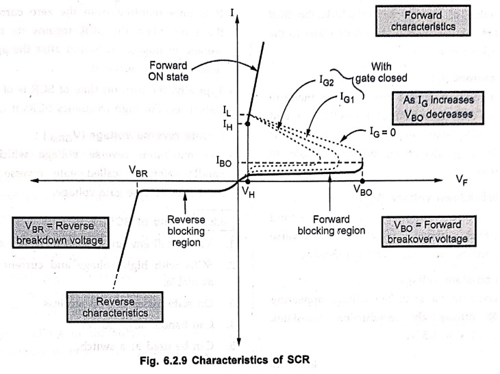
•
The characteristics are divided into two sections:
1. Forward characteristics :
•
It shows a forward blocking region, when IG = 0. It also shows that
when forward voltage increases upto VBO, the SCR turns ON and high
current results. The drop across SCR reduces suddenly which is now the ohmic
drop in the four layers. The current must be limited only by the external
resistance in series with the device.
•
It also shows that, if gate bias is used then as gate current increases, less
voltage is required to turn ON the SCR.
•
If the forward current falls below the level of the holding current IH,
then depletion region begins to develop around J2 and device goes
into the forward blocking region.
•
When SCR is turned ON from OFF state, the resulting forward current is called
latching current IL. The latching current is slightly higher than
the holding current.
2. Reverse
characteristics :
•
If the anode to cathode voltage is reversed, then the device enters into the
reverse blocking region. The current is negligibly small and practically
neglected.
•
If the reverse voltage is increased, similar to the diode, at a particular
value avalanche breakdown occurs and a large current flows through the device.
This is called reverse breakdown and the voltage at which this happens is
called reverse breakdown voltage VBR.
•
The forward breakover voltage is greater than reverse breakover voltage.
5. SCR Parameters
1. Forward breakover
voltage (VBO):
It
is the voltage above which the SCR enters the conduction region ('ON' state).
The The forward breakdown voltage is dependent on the gate bias.
2. Holding current (IH):
It
is that value of current below which the SCR switches from the conduction state
(ON state) to the forward blocking state.
3. Latching current (IL)
:
This
is the minimum current flowing from anode to cathode when SCR goes from OFF to
ON state and remains in ON state even after gate bias is removed. It is greater
than, but very close to holding current.
4. Reverse breakdown
voltage (VBR):
It
is the reverse voltage (Anode‒negative and cathode‒positive) above which the
reverse breakdown occurs, breaking J1 and J3 junctions.
5. Maximum on‒state
voltage:
It
is the maximum value of the voltage appearing across SCR during the conduction
(on‒state). Typically, it is 1 V to 1.5 V.
6. Current rating:
It
is the maximum current carrying ability of the SCR.
7. Minimum gate trigger
current (IGTmin)
The
minimum value of gate current which can trigger SCR is defined as IGTmin'.
8. Maximum gate current
(IGTmax):
It
is the peak value of gate current which must not be exceeded to avoid damage to
the SCR.
9. Gate power loss (PG):
It
is the mean power loss due to gate current between the gate and the main
terminal.
10. Turn on time (ton):
The
time required by SCR to reach full conduction after triggering is called 'turn
on time'.
The
turn on time consists of: i) Time required for charging gate to cathode
capacitance and ii) Time required for reaching latching current value.
Typically,
turn on time of SCR is of the order of 2‒4 μsec.
11. Turn off time (toff):
It
is time required from the zero current point to the time when the SCR regains
its full blocking voltage in positive direction after the application of
reverse voltage across it.
Typically,
the turn off time of SCR is of the order of 10‒50 μsec. For high frequency SCRS
it is 10‒20 μsec.
12. Gate reverse
voltage (VGRM):
The
maximum reverse voltage which gate can handle safely is called gate reverse
voltage or maximum reverse gate voltage.
6. Merits of SCR
1.
Very small amount of gate drive is required.
2.
SCRS with high voltage and current ratings are available.
3.
On state losses of SCR are less.
4.
Can handle large power
5.
Can be used as a switch.
6.
Easy to turn on.
7.
Can be easily protected with a fuse.
7. Demerits of SCR
1.
Gate has no control, once SCR is turned on.
2.
External circuits are required for turning it off.
3.
Operating frequencies are low.
4.
Additional protection circuits are required.
5.
Conducts only in one direction hence controls power during only one half cycle
of a.c. input.
8. Applications of SCR
1.
Controlled rectifiers.
2.
A.C. voltage stabilizers.
3.
D.C. to D.C. converters called choppers.
4.
D.C. to A.C. converters called inverters.
5.
Dimmerstats to control light intensity.
6.
For speed control schemes of d.c. and a.c. motors Ercalled drives.
7.
As a switch.
8.
Heater control circuit.
9.
In protection circuits.
9. SCR Crowbar Circuit
•
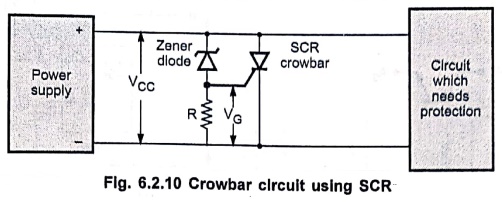
Crowbar circuits provide protection against over voltage conditions for entire
circuit. Fig. 6.2.10 shows crowbar circuit using SCR.
•
The zener diode in the circuit is selected such that at normal output voltage
it acts as an open switch. This is because Vcc is less than the breakdown
voltage of zener diode. Hence voltage across R is zero and SCR remains open.
•
When output voltage of the supply increases than the normal supply voltage by
any reason, the zener diode conducts and a voltage appears across R. This
voltage is sufficient to turn ON the SCR.
•
The conduction of SCR reduces the voltage drop across it and thus protects the
circuit from large over voltage.
•
As the turning ON of SCR is very fast, the instantaneous protection against the
high voltage is provided to the load.
Review Questions
1. Explain the construction of SCR.
2. Enumerate the structure of a SCR, with a two transistor model
derive an expression for anode current (IA) Also indicate its V‒I
characteristics.
3. Explain the working principle of SCR and its V‒I
characteristics.
4. Draw and explain the operation of SCR using two transistor
equivalent circuit.
5. Derive the expression for the anode current from the two
transistor model of SCR.
6. Draw and explain the characteristics of SCR.
7. Define the following with respect to SCR:
i. Forward breakover voltage ii. Holding current iii. Latching
current iv. Reverse breakdown voltage.
8. State the various specifications of SCR.
9. State the merits of SCR.
10. State the demerits of SCR.
11. State the various applications of SCR.
12. Explain the operation, characteristics and applications of
SCR.
Electron Devices: Chapter 6: Thyristors UJT and Optoelectronic Devices : Tag: electronics : Types of Construction, Working Principle, Two Transistor Model, Characteristics, Symbol, Equivalent Circuit, Parameters, Merits, Demerits, Applications, Crowbar Circuit - Silicon Controlled Rectifier (SCR)
Electron Devices: Chapter 6: Thyristors UJT and Optoelectronic Devices
Under Subject

Electron Devices
EC25C01 2nd Semester ECE Dept | 2025 Regulation | 2nd Semester 2025 Regulation
Related Subjects

English Essentials II
EN25C02 2nd Semester | 2025 Regulation | 2nd Semester 2025 Regulation

Tamils and Technology தமிழர்களும் தொழில்நுட்பமும்
UC25H02 2nd Semester | 2025 Regulation | 2nd Semester 2025 Regulation

Linear Algebra
MA25C02 2nd Semester | 2025 Regulation
Electron Devices
EC25C01 2nd Semester ECE Dept | 2025 Regulation | 2nd Semester 2025 Regulation

Data Structures using CPlusPlus
CS25C05 2nd Semester ECE Dept | 2025 Regulation | 2nd Semester 2025 Regulation

Circuits and Network Analysis
EC25C02 2nd Semester ECE Dept | 2025 Regulation | 2nd Semester 2025 Regulation

Re-Engineering for Innovation
ME25C05 2nd Semester | 2025 Regulation | 2nd Semester 2025 Regulation

Engineering Drawing - Laboratory
ME25C01 2nd Semester | 2025 Regulation | 2nd Semester 2025 Regulation

Data Structures using CPlusPlus - Laboratory
CS25C05 2nd Semester ECE Dept | 2025 Regulation | 2nd Semester 2025 Regulation

Devices and Circuits Laboratory
EC25C03 2nd Semester ECE Dept | 2025 Regulation | 2nd Semester 2025 Regulation