Electron Devices: Chapter 6: Thyristors UJT and Optoelectronic Devices
Light Emitting Diode (LED)
Construction, Working Principle, Operation, Symbol, Equivalent Circuit, Characteristics, Applications, Advantages, Disadvantages, Comparison, Example Solved Problems

Questions: 1. Enumerate the construction and operation of LED. 2. Explain the working principle of LED. 3. State the materials used in LED. 4. Explain the output characteristics of LED. 5. State the advantages of LED. 6. State the applications of LED. 7. State the disadvantages of LED. 8. Compare LED with P‒N junction diode.
Light
Emitting Diode (LED)
•
A diode which emits light when forward biased is called a Light Emitting Diode
(LED).
1. Construction of LED
•
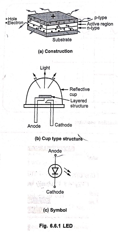
In LED three semiconductor layers on the substrate are used as shown in Fig.
6.6.1 (a). In between p type and n type region, there exists a region called
active region. This region is responsible for the emission of the light.
•
The LED emits light all the way around the layered structure. This layered
structure is placed in a tiny reflective cup so that the light gets reflected
towards the desired exit direction. This cup type structure is shown in Fig.
6.6.1 (b) while the symbol of the LED is shown in Fig. 6.6.1 (c).
2. Working Principle of LED
•
The LED works on the principle of electroluminescence.
•
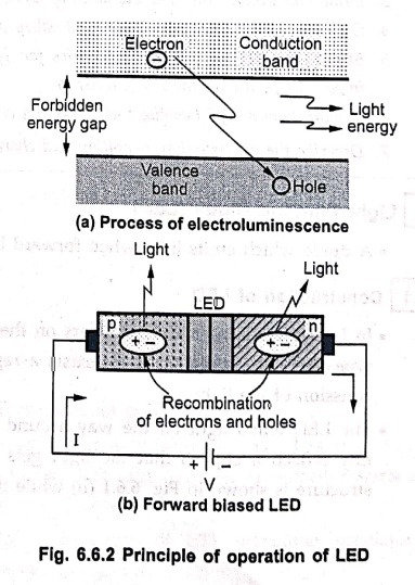
When a p‒n junction is forward biased, the electrons in n region cross the
junction and recombine with holes in p region.
•
The free electrons exist in the conduction band while the holes exist in the
valence band.
•
The energy level of free electrons is higher than the energy level of the
holes.
•
When electrons recombine with the holes, they move from conduction band to
valence band which is at lower energy level.
•
While moving, the additional energy is released by the free electrons which
appears in the form of light due to the special material used in the LED.
•
Practically when LED is forward biased, the holes from p region and electrons
from n region enter the active region between p and n regions. In the active
region recombination of electrons and holes take place and the energy is
released in the form of a light.
•
The energy released depends on the forbidden gap energy which determines the
wavelength and the colour of the emitted light.
•
Fig. 6.6.2 shows the principle of working of LED.
3. Internal Quantum Efficiency
•
For an ideal LED, the active region emits one photon for every electron
injected. Hence ideally the quantum efficiency of an LED is unity.
•
Practically the internal quantum efficiency of an LED is defined as the
fraction of the electrons that are injected to the depletion region which
results into photon getting produced.
•
In practical LED, all the power emitted from the active region is not emitted
to the free space. Some photons remain in the active region and never leave the
semiconductor.
•
The internal quantum efficiency is mathematically expressed as,
where
ηint
= Number of photons emitted from active region per second / Number of electrons
injected into LED per second
ηint = (Pint/ hν) / (I/e)
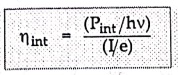
Pint
= Optical power emitted from the active region
I
= The injection current
e
= The charge on each electron
h
= Planck's constant
ν = Frequency of photon
4. External Quantum Efficiency
•
The photons must escape from the active region to the free space. But due to
physical structure and geometry of the material layers, the total internal
reflection occurs, which causes obstruction to escaping photons. Thus
extraction efficiency of an LED is defined as,
ηextraction = Number of photons
emitted into free space per second / Number of photons emitted from active
region per second
ηextraction = P/hν / Pint/hν
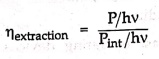
where
P = Optical power emitted into free space
•
Due to this, the external quantum efficiency of an LED is defined as the ratio
of photons emitted into free space to the electrons injected into LED.
ηext = Number of photons emitted
into free space per second / Number of electrons injected into LED per second
ηext = (P/hv) / (I/e)
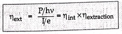
= ηint × ηextraction
•
Thus external quantum efficiency gives the indication of number of useful light
particles to the number of injected charge particles.
5. Materials of LED
•
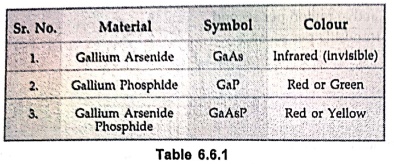
The materials which are the mixtures of gallium, arsenic and phosphorus, are
used in LED to obtain different colour of light.
•
The colour of light depends on wavelength which depends on the forbidden energy
gap value.
•
The various materials and colour obtained are given in Table 6.6.1.
6. LED Voltage and Current
•
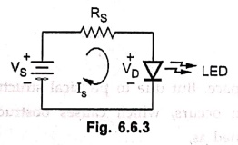
Consider a source connected to LED and resistor as shown in Fig. 6.6.3.
•
Due to RS the current IS gets limited.
•
If VD is the drop across LED then, applying KVL,
VS
= ISRS + VD
i.e.
IS
= [ VS‒VD ] / RS
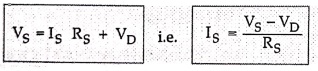
……….LED current
•
When forward biased, VD is about 1.5 V to 2.5 V.
•
Practically current range of IS is 10 to 70 mA.
•
If not provided, VD is assumed as 2 V.
7. Output Characteristics of LED
•
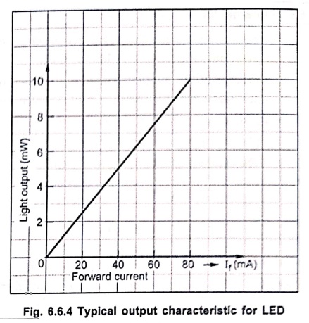
The amount of power output translated into light is directly proportional to
the forward current If. More the forward current If, the
greater is the output for of forward current light. The graph of forward current
and output light and output light in mW is shown in Fig. 6.6.4. This is called
output characteristics for LED.
8. Advantages of LED
•
The various advantages of LED are,
1.
LEDs are small in size, and hence can be regarded as point source of light.
Because of their small size, several thousand LEDs can be packed in one sq.
metre area.
2.
The brightness of light emitted by LED depends on the current flowing through
LED. Hence the brightness of light can be smoothly controlled by varying the
current. This makes possible to operate LED displays under different ambient
lighting conditions.
3.
LEDs are fast operating devices. They can be turned on and off in time less
than 1 microsecond.
4.
The LEDs are light in weight.
5.
The LEDs are available in various colours.
6.
The LEDs have long life.
7.
The LEDs are cheap and readily available.
8.
The LEDs are easy to interface with various other electronic circuits.
9.
Some LEDs radiate infrared light which is invisible but still useful in some
applications like burglar alarm systems.
9. Applications of LED
•
The various applications of LED are,
1.
All kinds of visual displays i.e. seven segment displays and alpha numeric
displays. Such displays are commonly used in the watches and calculators.
2.
In the optical devices such as optocouplers.
3.
As on‒off indicator in various types of electronic circuits.
4.
Some LEDs radiate infrared light which is invisible. But such LEDs are useful
in remote controls and applications like burglar alarm.
10. Disadvantages of LED
The
various disadvantages of LED are,
1.
It draws considerable current requiring frequent replacement of battery in low
power battery operated devices.
2.
Luminous efficiency of LEDs is low which is about 1.5 lumen/watt.
3.
The characteristics are affected by temperature.
4.
Need large power for the operation compared to normal p‒n junction diode.
11. Comparison of LED with P‒N Junction Diode
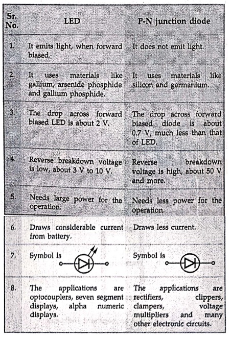
LED
1.
It emits light, when forward biased.
2.
It uses materials like gallium, arsenide phosphide and gallium phosphide.
3.
The drop across forward blased LED is about 2 V.
4.
Reverse breakdown voltage is low, about 3 V to 10 V.
5.
Needs large power for the operation.
6.
Draws considerable current from battery.
7. Symbol is
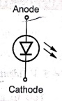
8.
The applications are optocouplers, seven segment displays, alpha numeric
displays.
P‒N junction diode
1.
It does not emit light.
2.
It uses materials like silicon and germanium.
3.
The drop across forward biased diode is about 0.7 V much less than that of LED.
4.
Reverse breakdown voltage is high, about 50 V and more.
5.
Needs less power for the operation.
6.
Draws less current.
7.
Symbol is
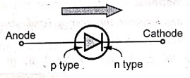
8.
The applications are rectifiers, clippers, clampers, voltage multipliers and
many other electronic circuits.
Ex. 6.6.1: What is the current through LED
shown in Fig. 6.6.5.
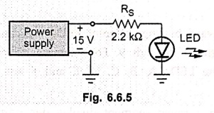
Solution: :
VS
= 15 V, RS = 2.2 kΩ
Assume
LED voltage drop as VD = 2 V
IS = (VS‒VD) /
RS
= (15‒2) / 2.2×103
= 5.91 mA
…………. LED current
Review Questions
1. Enumerate the construction and operation of LED.
2. Explain the working principle of LED.
3. State the materials used in LED.
4. Explain the output characteristics of LED.
5. State the advantages of LED.
6. State the applications of LED.
7. State the disadvantages of LED.
8. Compare LED with P‒N junction diode.
Electron Devices: Chapter 6: Thyristors UJT and Optoelectronic Devices : Tag: electronics : Construction, Working Principle, Operation, Symbol, Equivalent Circuit, Characteristics, Applications, Advantages, Disadvantages, Comparison, Example Solved Problems - Light Emitting Diode (LED)
Electron Devices: Chapter 6: Thyristors UJT and Optoelectronic Devices
Under Subject

Electron Devices
EC25C01 2nd Semester ECE Dept | 2025 Regulation | 2nd Semester 2025 Regulation
Related Subjects

English Essentials II
EN25C02 2nd Semester | 2025 Regulation | 2nd Semester 2025 Regulation

Tamils and Technology தமிழர்களும் தொழில்நுட்பமும்
UC25H02 2nd Semester | 2025 Regulation | 2nd Semester 2025 Regulation

Linear Algebra
MA25C02 2nd Semester | 2025 Regulation
Electron Devices
EC25C01 2nd Semester ECE Dept | 2025 Regulation | 2nd Semester 2025 Regulation

Data Structures using CPlusPlus
CS25C05 2nd Semester ECE Dept | 2025 Regulation | 2nd Semester 2025 Regulation

Circuits and Network Analysis
EC25C02 2nd Semester ECE Dept | 2025 Regulation | 2nd Semester 2025 Regulation

Re-Engineering for Innovation
ME25C05 2nd Semester | 2025 Regulation | 2nd Semester 2025 Regulation

Engineering Drawing - Laboratory
ME25C01 2nd Semester | 2025 Regulation | 2nd Semester 2025 Regulation

Data Structures using CPlusPlus - Laboratory
CS25C05 2nd Semester ECE Dept | 2025 Regulation | 2nd Semester 2025 Regulation

Devices and Circuits Laboratory
EC25C03 2nd Semester ECE Dept | 2025 Regulation | 2nd Semester 2025 Regulation