Electron Devices: Chapter 6: Thyristors UJT and Optoelectronic Devices
Unijunction Transistor (UJT)
Construction, Working Principle, Symbol, Equivalent circuit, VI characteristics, Applications

Questions: 1. Explain the basic construction and working of UJT. Draw its equivalent circuit. 2. Explain the equivalent circuit and define intrinsic stand off ratio of UJT. 3. Draw and explain the characteristics of UJT. 4. Define negative resistance region and valley point current with respect to UJT. 5. Sketch the UJT emitter characteristics for IB2 = 0, VBB = 20 V and VBB = 5 V. Identify each region and important points on the characteristics. 6. Explain how a UJT functions as relaxation oscillator. 7. Describe the construction, operation and characteristics of UJT.
Unijunction
Transistor (UJT)
•
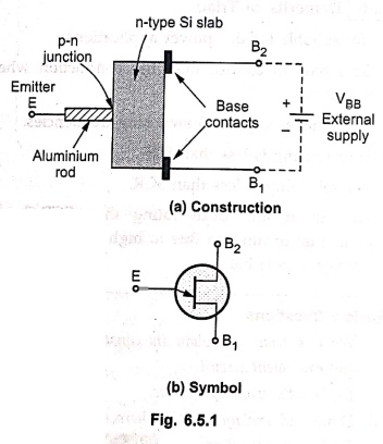
It is a three terminal device having two layers. It consists of lightly doped n
type silicon slab to which aluminium rod is alloyed at the one end with a p
type material, forming a p‒n junction.
•
At other end of slab, two base contacts B1 and B2 are
attached. The third terminal emitter E is taken out from aluminium rod.
•
Fig. 6.5.1 shows the construction and symbol of UJT.
•
It has only one p‒n junction p‒n junction hence called unijunction.
•
The p‒n junction can be treated as a diode D while internal resistances of two
bases are denoted as RB1 and RB2. The resistance RB1
is greater than RB2.
•
When emitter diode is not conducting, the resistance between two bases is
called interbase resistance given by RBB = RB1 + RB2.
• Fig. 6.5.2 shows the equivalent circuit of UJT.
•
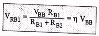
When IE = 0, then the voltage drop across RB1 is given
by,
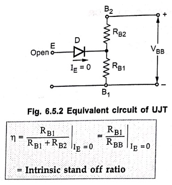
= Intrinsic stand off ratio
•
The value of η is between 0.5 to 0.8.
Working of UJT:
•
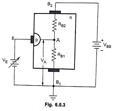
The supply voltage VBB is connected between B1 and B2
while variable emitter voltage VE is applied to emitter. This is
shown in Fig. 6.5.3.
•
The VE is used to forward bias the diode. The drop across diode is VD.'
•
The potential of A is decided by η and is equal to η VBB.
Case 1: VE
< VA
•
As long as VE is less than VA, the p‒n junction is reverse
biased. Hence emitter current IE will not flow. Thus UJT is said to
be OFF.
Case 2: VE
> VP
•
The diode drop VD is generally between 0.3 to 0.7 V. Hence we can
write,
VP
= VA + VD = ηVBB
+ VD
•
When VE becomes equal to or greater than VP the p‒n
junction becomes forward biased and current IE flows.
•
Due to this the charge carriers are injected in the RBI region of
the bar.
•
Due to these additional charge carriers, the conductivity of the RB1
region increases i.e. resistance and due to which the drop across it also
decreases.
•
This makes the p‒n junction more forward biased which further increases the
current and more charge carriers are injected.
•
The current IE is increases to a value determined by the source
resistance.
•
Under these conditions, the UJT is said to be ON and remains in this condition
till the input is open or the current IE gets reduced to very low
value.
1. UJT Charateristics
•
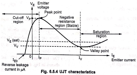
The graph of emitter current against emitter voltage plotted for a particular
value of VBB is called the characteristics of UJT.
•
For a particular fixed fixed value of VBB such characteristics is
shown in Fig. 6.5.4.
•
The characteristics can be divided into three main regions which are,
1. Cut‒off region:
The emitter voltage VE is less than VP and the p‒n
junction is reverse biased. A small amount of reverse saturation current IEO
flows through the device, which is negligibly small of the order of μA. This
condition remains till the peak point.
2. Negative resistance
region: When the emitter voltage VE
becomes equal to VP the p‒n junction becomes forward biased and IE
starts flowing. The voltage across the device decreases in this region, though
the current through the device increases. Hence the region is called negative
resistance region. This decreases the resistance RB1. This region is
stable and used in many applications. This region continues till valley point.
3. Saturation region:
Increase in IE further valley point current IV drives the
device in the saturation region. The voltage corresponding to valley point is
called valley point voltage denoted as VV. In this region, further
decrease in voltage does not take place. The characteristic is similar to that
of a semiconductor diode, in this region.
• The active region i.e. negative resistance region, the holes which are large in number on p‒side, get injected into n‒side. This causes increase in free electrons in the n‒type slab. This increases the conductivity i.e. decreases the resistivity. Hence the resistance RB1 decreases in this region.
•
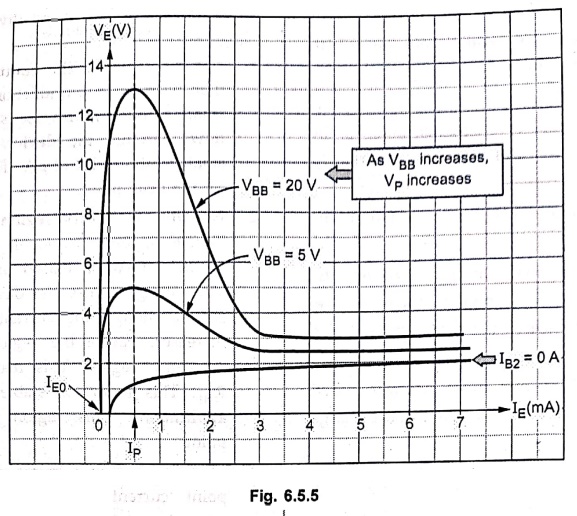
As the VBB increases, the potential VP corresponding to
peak point will increase.
•
The typical UJT emitter characteristics for IB2 = 0, VBB
= 20 V and VBB = 5V are shown in Fig. 6.5.5.
2. Applications of UJT
•
The various applications of UJT are,
1.
Triggering of other devices like SCR.
2.
In a sawtooth waveform generator.
3.
In a relaxation oscillator.
4.
In timing circuits.
5.
In automobile ignition circuits.
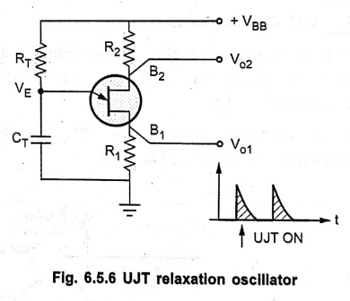
UJT relaxation
oscillator: Fig. 6.5.6 shows the circuit of UJT relaxation
oscillator.
•
R1 and R2 are biasing resistors. RT and CT
decide the oscillating rate.
•
The value of RT is so selected that UJT operates in negative
resistance region.
•
CT gets charged to VBB through RT.
•
When its voltage is more than VP, UJT fires. Then Ст Cr starts discharging
through RB1 + R1. This discharge is very fast due to
small R1.
•
This produces pulse across R1.
•
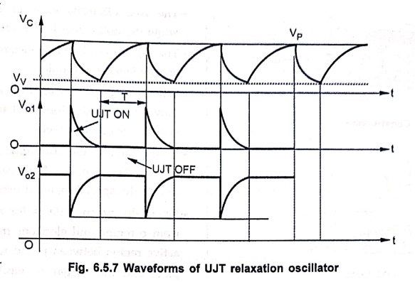
Then capacitor voltage becomes less than VV, UJT becomes OFF and
charging of capacitor starts again and cycle repeats.
•
The waveforms of UJT relaxation oscillator are shown in Fig. 6.5.7.
Review Questions
1. Explain the basic construction and working of UJT. Draw its
equivalent circuit.
2. Explain the equivalent circuit and define intrinsic stand off
ratio of UJT.
3. Draw and explain the characteristics of UJT.
4. Define negative resistance region and valley point current
with respect to UJT.
5. Sketch the UJT emitter characteristics for IB2 = 0,
VBB = 20 V and VBB = 5 V. Identify each region and important
points on the characteristics.
6. Explain how a UJT functions as relaxation oscillator.
7. Describe the construction, operation and characteristics of
UJT.
Electron Devices: Chapter 6: Thyristors UJT and Optoelectronic Devices : Tag: electronics : Construction, Working Principle, Symbol, Equivalent circuit, VI characteristics, Applications - Unijunction Transistor (UJT)
Electron Devices: Chapter 6: Thyristors UJT and Optoelectronic Devices
Under Subject

Electron Devices
EC25C01 2nd Semester ECE Dept | 2025 Regulation | 2nd Semester 2025 Regulation
Related Subjects

English Essentials II
EN25C02 2nd Semester | 2025 Regulation | 2nd Semester 2025 Regulation

Tamils and Technology தமிழர்களும் தொழில்நுட்பமும்
UC25H02 2nd Semester | 2025 Regulation | 2nd Semester 2025 Regulation

Linear Algebra
MA25C02 2nd Semester | 2025 Regulation
Electron Devices
EC25C01 2nd Semester ECE Dept | 2025 Regulation | 2nd Semester 2025 Regulation

Data Structures using CPlusPlus
CS25C05 2nd Semester ECE Dept | 2025 Regulation | 2nd Semester 2025 Regulation

Circuits and Network Analysis
EC25C02 2nd Semester ECE Dept | 2025 Regulation | 2nd Semester 2025 Regulation

Re-Engineering for Innovation
ME25C05 2nd Semester | 2025 Regulation | 2nd Semester 2025 Regulation

Engineering Drawing - Laboratory
ME25C01 2nd Semester | 2025 Regulation | 2nd Semester 2025 Regulation

Data Structures using CPlusPlus - Laboratory
CS25C05 2nd Semester ECE Dept | 2025 Regulation | 2nd Semester 2025 Regulation

Devices and Circuits Laboratory
EC25C03 2nd Semester ECE Dept | 2025 Regulation | 2nd Semester 2025 Regulation