Electron Devices: Chapter 5: Field Effect Transistors
Field Effect Transistors: Important Example Solved Problems
Electron Devices
Electron Devices: Chapter 5: Field Effect Transistors: Anna University Solved Problems, Assignment Problems and Important Solved Problems
Electron
Devices
Chapter
5: Field Effect Transistors
Important
Example Solved Problems
The Pinch‒off
Voltage VP
Ex. 1: For an n‒channel silicon
FET, find the pinch‒off voltage and the channel half‒width.
Assume: a = 3 × 10‒6
m, ND = 1021 electrons/m2, VGS= 1/2
VP, ID = 0 and relative dielectric constant of silicon =
12.
Solution:
Since
relative dielectric constant of silicon is 12 we have ε = 12ε0.
Using values of q and ε0 we have
VP
= [ 1.6×10‒19×1021×(3×10‒6)2 ] / [2×12×(8.85×10‒12)]
= 6.8 V
From
equation (5.6.6) we have
VGS = (1 ‒ (b/a))2 VP
(1
‒ (b/a))2 = VGS / VP = 1/2
1 ‒ (b/a) = 0.707
b = (1 ‒ 0.707)a
=
(0.293) (3 × 10⁻⁶) = 0.879 m
This
result shows that the channel width is reduced to about one‒third its value for
VGS
= ½ VP
Ex. 2: Assume that the p+n
junction of a uniformly doped silicon n channel JFET at T = 300 K has doping
concentrations of Na =1018 cm and Nd = 1016
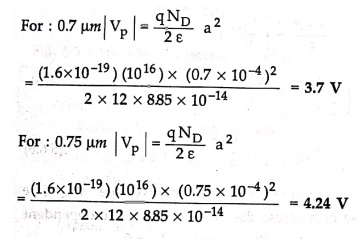
cm−3. Assume that the metallurgical channel thickness a is 0.7 μm
Calculate the pinch off voltage. Also calculate pinch‒off voltage if the
metallurgical channel thickness a is 0.75 μm.
Solution:
Here
all quantities are in centimeters instead of meters. Channel thickness a = 0.7 μm
= 0.7×10‒4 cm. The internal pinch off voltage is given by
Characteristics
Parameters of JFET (Transconductance)
Ex. 3: For JFET, if IDSS
= 20 mA, VGS(off) = − 5 V, and gmo = 4 mS or mA/V.
Determine the transconductance for VGS = ‒ 4 V, and find ID
at this point.
Solution:
From
equation (5.7.2) we have,

= 4×10‒3 × 0.2 = 0.8 mS
We
have,

= 20×10‒3 × 0.04 = 0.8 mA
n‒Channel E‒MOSFET - Current
Equation
Ex. 4: For N‒EMOSFET VT
= 0.7 V, W= 30 μm, L=5 μm, μn = 650 cm2/V‒S, tox
= 450 A (450 × 10‒8). εox = 3.9 × 8.85 × 10‒14
F/cm
Assume transistor is biased
in saturation region:
i) Determine drain current
when VGS = 2VT. ii) If tox is doubled, find
new K.
Solution:
i)
W = 30 μm = 30 × 10‒6 m = 30 × 10‒4 cm
L
= 5 μm = 5 × 10‒6 m = 5 × 10‒4 cm
K
= Wμnεox / 2Ltox
=
[ (30×10‒4) (650) (3.9×8.85×10‒14) ] / [ 2(5×10‒4)(450×10−8)
]
=
0.1495 mA/V2
VGS
= 2 VT = 2 × 0.7 = 1.4 V
iD
= K (VGS ‒ VT)2 = (0.1495) (1.4 ‒ 0.7)2
=
0.0732 mA
ii)
For tox = 2 × 450 × 10‒8 = 900 × 10‒8
K
= Wμnεox / 2Ltox
=
[ (30×10‒4) (650)
(3.9×8.85×10‒14) ] / [ 2(5×10‒4)(900×10‒8) ]
=
0.07475 mA/V2
Ex. 5: Evaluate the body effect
coefficient (γ) in a MOSFET with Na = 3×10¹⁶/cm3,
εr = 11.6 and ε0 = 8.854×10‒12 F/m and Cox
= 1.726×10‒7 F/cm2.
Solution::
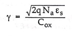
where
εS = εr × ε0
=
11.6×8.854×10‒12 F/m
=
11.6×8.854×10‒14 F/cm
γ = { √[2×(1.6×10‒19)×(3×1016)×(11.6×8.854×10−14)
] / [ 1.726×10‒7 ]
=
0.5753
Electron Devices: Chapter 5: Field Effect Transistors : Tag: electronics : Electron Devices - Field Effect Transistors: Important Example Solved Problems
Electron Devices: Chapter 5: Field Effect Transistors
Under Subject

Electron Devices
EC25C01 2nd Semester ECE Dept | 2025 Regulation | 2nd Semester 2025 Regulation
Related Subjects

English Essentials II
EN25C02 2nd Semester | 2025 Regulation | 2nd Semester 2025 Regulation

Tamils and Technology தமிழர்களும் தொழில்நுட்பமும்
UC25H02 2nd Semester | 2025 Regulation | 2nd Semester 2025 Regulation

Linear Algebra
MA25C02 2nd Semester | 2025 Regulation
Electron Devices
EC25C01 2nd Semester ECE Dept | 2025 Regulation | 2nd Semester 2025 Regulation

Data Structures using CPlusPlus
CS25C05 2nd Semester ECE Dept | 2025 Regulation | 2nd Semester 2025 Regulation

Circuits and Network Analysis
EC25C02 2nd Semester ECE Dept | 2025 Regulation | 2nd Semester 2025 Regulation

Re-Engineering for Innovation
ME25C05 2nd Semester | 2025 Regulation | 2nd Semester 2025 Regulation

Engineering Drawing - Laboratory
ME25C01 2nd Semester | 2025 Regulation | 2nd Semester 2025 Regulation

Data Structures using CPlusPlus - Laboratory
CS25C05 2nd Semester ECE Dept | 2025 Regulation | 2nd Semester 2025 Regulation

Devices and Circuits Laboratory
EC25C03 2nd Semester ECE Dept | 2025 Regulation | 2nd Semester 2025 Regulation