Electron Devices: Chapter 5: Field Effect Transistors
Enhancement MOSFET (E‒MOSFET)
Construction, Operation, Characteristics, Circuit Diagram, Parameters, Type, Symbols, Example Solved Problems

Questions: 1. Define threshold voltage. 2. Define pinchoff voltage. 3. Sketch and explain the construction of N‒channel enhancement type MOSFET. Give also its symbol. 4. Explain the operation of an enhancement type MOSFET. 5. Describe, with suitable sketches, the operation and characteristics (transfer, drain) of the N‒channel enhancement type MOSFET. 6. With the help of suitable diagrams explain the working of different types of MOSFET. 7. Draw a circuit diagram of the cross section of a enhancement MOSFET. Also discuss the drain and transfer characteristics for EMOSFET. 8. Explain the concept of threshold voltage in a MOSFET. 9. Discuss the characteristics of MOSFET. 10. Describe the working and characteristics of MOSFET, D MOSFET and E MOSFET. 11. Discuss your understanding on MOSFET detailing the types, construction and characteristics.
Enhancement
MOSFET (E‒MOSFET)
•
This type of MOSFET operates only in the enhancement mode and has no depletion
mode. It differs in construction from the depletion MOSFET in that it has no
physical channel.
1. Construction of n‒channel E‒MOSFET
•
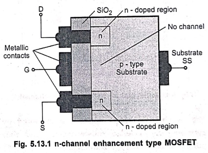
Fig. 5.13.1 shows the basic construction of n‒channel enhancement type MOSFET.
•
Like, depletion type MOSFET, two highly doped n‒regions are diffused into a
lightly doped p‒type substrate.
•
The source and drain are taken out through metallic contacts to n‒doped regions
as shown in Fig. 5.13.1.
•
But the channel between two n‒regions is absent in the enhancement type MOSFET.
•
The SiO2 layer is still present to isolate the gate metallic
platform from the region between the drain and source, but now it is simply
separated from a section of the p‒type material.
2. Operation, Characteristics and Parameters of n‒Channel E‒MOSFET
•
On application of drain to source voltage VDS and keeping gate to
source voltage zero by directly connecting gate terminal to the source
terminal, practically zero current flows‒quite different from the depletion
type MOSFET and JFET.
•
If we increase magnitude of VGS in the positive direction, the
concentration of electrons near the SiO2 surface increases.
•
At a particular value of VGS there is a measurable current flow
between drain and source. This value of VGS is called threshold voltage denoted by VT.
•
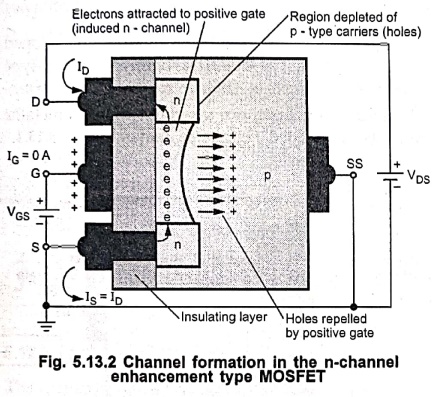
Thus, we can say that in an enhancement type n‒channel MOSFET, a positive gate
voltage above a threshold value induces a channel and hence the drain current
by creating a thin layer of negative charges in the substrate region adjacent
to the SiO2 layer, as shown in Fig. 5.13.2.
•
The conductivity of the channel is enhanced by increasing the gate to source
voltage and thus pulling more electrons into the channel.
•
For any voltage below the threshold value, there is no channel.
•
Since the channel does not exist with VGS = 0 V and
"enhanced" by the application of a positive gate to source voltage,
this type of MOSFET is called an enhancement type MOSFET.
•
Fig. 5.13.3 shows the drain characteristics of an n‒channel enhancement type
MOSFET. Looking at Fig. 5.13.3 we can say that as VGS increases
beyond the threshold level, the density of free carriers (electrons) in the
induced channel increases, increasing the drain current. However, at some point
of VDS, for constant VGS, the drain current reaches a
saturation level.
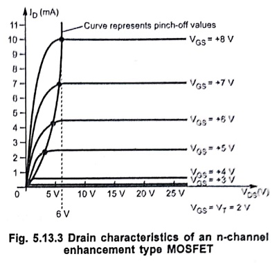
Fig. 5.13.3 Drain
characteristics of an n‒channel enhancement type MOSFET
•
The value of VDS at this point is known as pinch‒off voltage (VP).
The levelling off of ID is due to a pinch‒off process. Fig. 5.13.4
shows pinch off process for n‒channel enhancement type MOSFET.
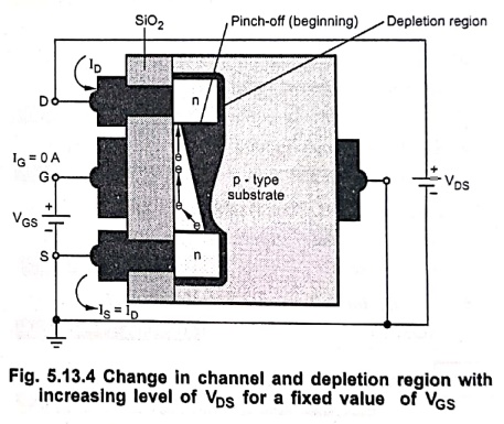
Fig. 5.13.4 Change in
channel and depletion region with increasing level of VDS for a
fixed value of VGS
•
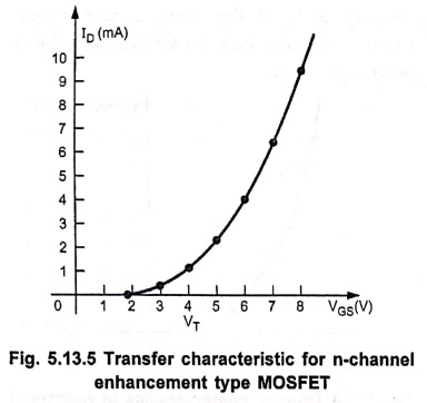
Fig. 5.13.5 shows the transfer characteristic for n‒channel enhancement type
MOSFET.
•
This characteristic is quite different from characteristic that we we obtained
for JFET and depletion type MOSFET. For an n‒channel enhancement type MOSFET it
is now totally in the positive VGS
region and as we know ID does not flow until VGS = VT.
•
For VGS > VT the relationship between drain current
and VGS is nonlinear and it is given as
ID
= K(VGS ‒ VT )2
……….(5.13.1)
•
The K term is a constant that is a function of the construction of the device.
The value of K can be determined from equation,
K
= ID(ON) / (VGS(ON) ‒ VT )2
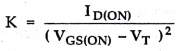
………(5.13.2)
•
The parameter K is called conduction parameter. It is given by K = WμnCOX
/ 2L
•
Where Cox is the oxide capacitance per unit area. The capacitance is
given by
COX
= εox / tox
where
tox is the oxide thickness and εox is the oxide
permittivity.
•
The parameter μn is the mobility of the electrons in the inversion
layer.
•
The parameter W is the channel width and parameter L is the channel length.
Ex. 5.13.1: For N‒EMOSFET VT = 0.7
V, W= 30 μm, L=5 μm, μn = 650 cm2/V‒S, tox =
450 A (450 × 10‒8). εox = 3.9 × 8.85 × 10‒14
F/cm
Assume transistor is
biased in saturation region:
i) Determine drain
current when VGS = 2VT. ii) If tox is doubled,
find new K.
Solution:
i)
W = 30 μm = 30 × 10‒6 m = 30 × 10‒4 cm
L
= 5 μm = 5 × 10‒6 m = 5 × 10‒4 cm
K
= Wμnεox / 2Ltox
=
[ (30×10‒4) (650) (3.9×8.85×10‒14) ] / [ 2(5×10‒4)(450×10−8)
]
=
0.1495 mA/V2
VGS
= 2 VT = 2 × 0.7 = 1.4 V
iD
= K (VGS ‒ VT)2 = (0.1495) (1.4 ‒ 0.7)2
=
0.0732 mA
ii)
For tox = 2 × 450 × 10‒8 = 900 × 10‒8
K
= Wμnεox / 2Ltox
=
[ (30×10‒4) (650)
(3.9×8.85×10‒14) ] / [ 2(5×10‒4)(900×10‒8) ]
=
0.07475 mA/V2
Ex. 5.13.2: Evaluate the body effect
coefficient (γ) in a MOSFET with Na = 3×10¹⁶/cm3,
εr = 11.6 and ε0 = 8.854×10‒12 F/m and Cox
= 1.726×10‒7 F/cm2.
Solution::
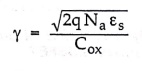
where
εS = εr × ε0
=
11.6×8.854×10‒12 F/m
=
11.6×8.854×10‒14 F/cm
γ = { √[2×(1.6×10‒19)×(3×1016)×(11.6×8.854×10−14)
] / [ 1.726×10‒7 ]
=
0.5753
3. p‒channel Enhancement Type MOSFET
•
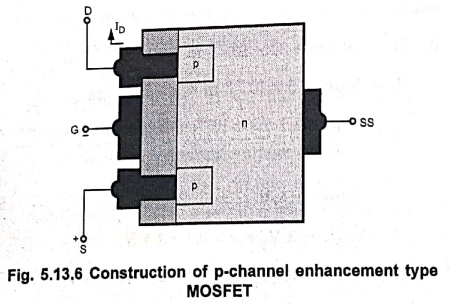
The construction of the p‒channel enhancement type MOSFET is exactly opposite
to that of n‒channel enhancement type MOSFET. Here, the substrate is of n‒type
and regions are of p‒type as shown in Fig. 5.13.6.6
•
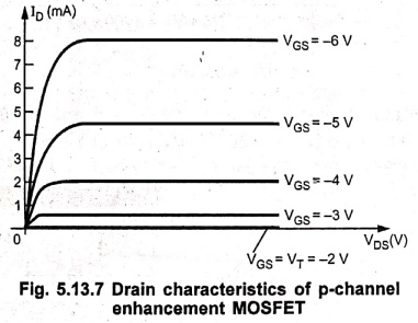
As shown in Fig. 5.13.7 voltage polarities and current directions are reversed.
•
The drain characteristics appear exactly as in the Fig. 5.13.7 but with VDS
with negative values, ID in opposite direction and VGS
having opposite polarities as shown in Fig. 5.13.7.
•
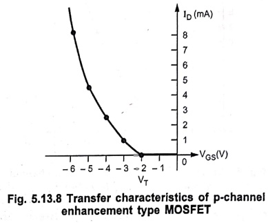
Fig. 5.13.8 shows the transfer characteristics of p‒channel enhancement type
MOSFET.
•
In the p‒channel enhancement type MOSFET, the transfer characteristic is a
mirror image about the ID axis (y axis) of the transfer
characteristics of n‒channel depletion type MOSFET, since the VGS is
negative.
E‒MOSFET symbols
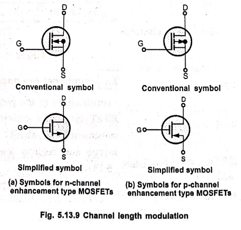
Fig.
5.13.9 shows graphic symbols for n and p‒channel enhancement type MOSFET.
Review
Questions
1. Define threshold voltage.
2. Define pinchoff voltage.
3. Sketch and explain the construction of N‒channel enhancement
type MOSFET. Give also its symbol.
4. Explain the operation of an enhancement type MOSFET.
5. Describe, with suitable sketches, the operation and
characteristics (transfer, drain) of the N‒channel enhancement type MOSFET.
6. With the help of suitable diagrams explain the working of
different types of MOSFET.
7. Draw a circuit diagram of the cross section of a enhancement
MOSFET. Also discuss the drain and transfer characteristics for EMOSFET.
8. Explain the concept of threshold voltage in a MOSFET.
9. Discuss the characteristics of MOSFET.
10. Describe the working and characteristics of MOSFET, D MOSFET
and E MOSFET.
11. Discuss your understanding on MOSFET detailing the types,
construction and characteristics.
Electron Devices: Chapter 5: Field Effect Transistors : Tag: electronics : Construction, Operation, Characteristics, Circuit Diagram, Parameters, Type, Symbols, Example Solved Problems - Enhancement MOSFET (E‒MOSFET)
Electron Devices: Chapter 5: Field Effect Transistors
Under Subject

Electron Devices
EC25C01 2nd Semester ECE Dept | 2025 Regulation | 2nd Semester 2025 Regulation
Related Subjects

English Essentials II
EN25C02 2nd Semester | 2025 Regulation | 2nd Semester 2025 Regulation

Tamils and Technology தமிழர்களும் தொழில்நுட்பமும்
UC25H02 2nd Semester | 2025 Regulation | 2nd Semester 2025 Regulation

Linear Algebra
MA25C02 2nd Semester | 2025 Regulation
Electron Devices
EC25C01 2nd Semester ECE Dept | 2025 Regulation | 2nd Semester 2025 Regulation

Data Structures using CPlusPlus
CS25C05 2nd Semester ECE Dept | 2025 Regulation | 2nd Semester 2025 Regulation

Circuits and Network Analysis
EC25C02 2nd Semester ECE Dept | 2025 Regulation | 2nd Semester 2025 Regulation

Re-Engineering for Innovation
ME25C05 2nd Semester | 2025 Regulation | 2nd Semester 2025 Regulation

Engineering Drawing - Laboratory
ME25C01 2nd Semester | 2025 Regulation | 2nd Semester 2025 Regulation

Data Structures using CPlusPlus - Laboratory
CS25C05 2nd Semester ECE Dept | 2025 Regulation | 2nd Semester 2025 Regulation

Devices and Circuits Laboratory
EC25C03 2nd Semester ECE Dept | 2025 Regulation | 2nd Semester 2025 Regulation