Electron Devices: Chapter 5: Field Effect Transistors
JFET: The Pinch-off Voltage
Questions: 1. Derive the expresion for pinch‒off voltage. 2. Important Example Solved Problems
The
Pinch‒off Voltage VP
•
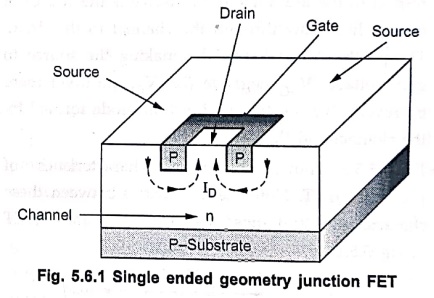
Fig. 5.6.1 shows a single‒ended‒geometry junction FET. Here, the substrate is
of p‒type material onto which an n‒type channel is epitaxially grown. A p‒type
gate is then diffused into the n‒type channel. In this device, a slab of n‒type
semiconductor is sandwiched between two layers of p‒type material, forming two
p‒n junctions.
•
Let us assume that the p‒type region is doped with NA acceptors per
cubic meter, n‒type region is doped with ND donors per cubic meter
and that the junction formed is abrupt.
•
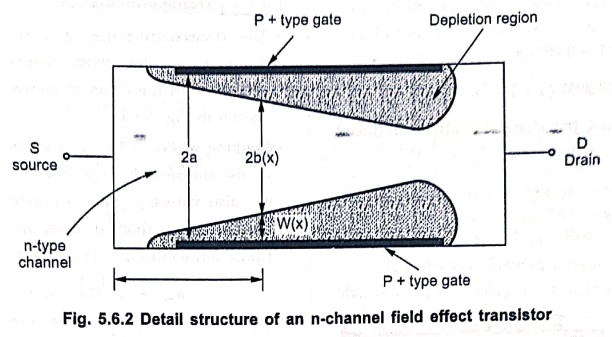
We know that, if NA >> ND we have WP
<< Wn and for the space‒charge width, Wn(x) = W(x)
at a distance x along the channel in Fig. 5.6.2.

…………... (5.6.1)
where
ε
: Dielectric constant of channel material
q
: Magnitude of electric charge
VO
: Junction contact potential at x
V(x):
Applied potential across space‒charge region at x and is a negative number for
an applied reverse bias
a ‒ b(x): Penetration W(x) of depletion region
into channel at a point x along channel
•
When the drain current is zero, b(x) and V(x) are independent of x and b(x) =
b. By substituting b(x) = b = 0 we have
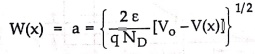
………… (5.6.2)
•
Now solving for V with assumption |V0| << |V| we obtain the
pinch‒off voltage VP (the diode reverse voltage that removes all the
free charge from the channel) as
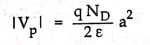
………… (5.6.3)
•
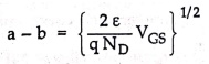
If we substitute VGS for VO ‒ V(x) and b(x) = b in equation
(5.6.1) we get,
………… (5.6.4)
•
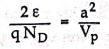
From equation (5.6.3) we have
………… (5.6.5)
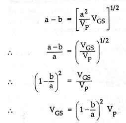
Substituting
equation (5.6.5) in equation (5.6.4) we get,
...(5.6.6)
•
This equation shows that the voltage VGS (the reverse bias across
the gate junction) is independent of distance along the channel if ID
= 0.
Ex. 5.6.1: For an n‒channel silicon FET,
find the pinch‒off voltage and the channel half‒width.
Assume: a = 3 × 10‒6
m, ND = 1021 electrons/m2, VGS= 1/2
VP, ID = 0 and relative dielectric constant of silicon =
12.
Solution:
Since
relative dielectric constant of silicon is 12 we have ε = 12ε0.
Using values of q and ε0 we have
VP
= [ 1.6×10‒19×1021×(3×10‒6)2 ] / [2×12×(8.85×10‒12)]
= 6.8 V
From
equation (5.6.6) we have
VGS = (1 ‒ (b/a))2 VP
(1
‒ (b/a))2 = VGS / VP = 1/2
1 ‒ (b/a) = 0.707
b = (1 ‒ 0.707)a
=
(0.293) (3 × 10⁻⁶) = 0.879 m
This
result shows that the channel width is reduced to about one‒third its value for
VGS
= ½ VP
Ex. 5.6.2: Assume that the p+n junction of a
uniformly doped silicon n channel JFET at T = 300 K has doping concentrations
of Na =1018 cm and Nd = 1016 cm−3.
Assume that the metallurgical channel thickness a is 0.7 μm Calculate the pinch
off voltage. Also calculate pinch‒off voltage if the metallurgical channel
thickness a is 0.75 μm.
Solution:
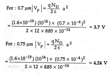
Here
all quantities are in centimeters instead of meters. Channel thickness a = 0.7 μm
= 0.7×10‒4 cm. The internal pinch off voltage is given by
Review
Question
1. Derive the expresion for pinch‒off voltage.
Electron Devices: Chapter 5: Field Effect Transistors : Tag: electronics : - JFET: The Pinch-off Voltage
Electron Devices: Chapter 5: Field Effect Transistors
Under Subject

Electron Devices
EC25C01 2nd Semester ECE Dept | 2025 Regulation | 2nd Semester 2025 Regulation
Related Subjects

English Essentials II
EN25C02 2nd Semester | 2025 Regulation | 2nd Semester 2025 Regulation

Tamils and Technology தமிழர்களும் தொழில்நுட்பமும்
UC25H02 2nd Semester | 2025 Regulation | 2nd Semester 2025 Regulation

Linear Algebra
MA25C02 2nd Semester | 2025 Regulation
Electron Devices
EC25C01 2nd Semester ECE Dept | 2025 Regulation | 2nd Semester 2025 Regulation

Data Structures using CPlusPlus
CS25C05 2nd Semester ECE Dept | 2025 Regulation | 2nd Semester 2025 Regulation

Circuits and Network Analysis
EC25C02 2nd Semester ECE Dept | 2025 Regulation | 2nd Semester 2025 Regulation

Re-Engineering for Innovation
ME25C05 2nd Semester | 2025 Regulation | 2nd Semester 2025 Regulation

Engineering Drawing - Laboratory
ME25C01 2nd Semester | 2025 Regulation | 2nd Semester 2025 Regulation

Data Structures using CPlusPlus - Laboratory
CS25C05 2nd Semester ECE Dept | 2025 Regulation | 2nd Semester 2025 Regulation

Devices and Circuits Laboratory
EC25C03 2nd Semester ECE Dept | 2025 Regulation | 2nd Semester 2025 Regulation