Electron Devices: Chapter 5: Field Effect Transistors
Characteristics of JFET
Questions: 1. Sketch and explain the drain characteristics for an n‒channel FET. 2. Draw a circuit diagram to obtain the drain characteristics for an n‒channel JFET. Thus draw drain characteristics and explain them. 3. Explain the drain characteristics for p‒channel FET. 4. Explain the transfer characteristics for n‒channel JFET. 5. Explain the transfer characteristics for p‒channel JFET. 6. What do you understand by 'pinch off voltages' and 'cut‒off voltages'? 7. Draw a circuit for obtaining drain and transfer characteristics for an n‒channel JFET. 8. Sketch a typical drain characteristic for an n‒channel JFET. Explain the shape of the characteristic and identify the regions. 9. Sketch the basic circuits for both N channel JFET and P‒channel JFET. 10. Sketch and explain the drain‒characteristics and transfer‒characteristics of P‒channel JFET. 11. When a FET acts as a voltage variable resistor? 12. Explain the four distinct regions of the output characteristics of the JFET. 13. Discuss the drain and transfer characteristics of JFETS.
Characteristics
of JFET
•
To understand electrical behaviour of a JFET, it is necessary to study the
interrelation of the current and voltages in JFET. These relationships can be
plotted graphically which are commonly known as the characteristics of JFET.
•
The important characteristics of JFET are drain characteristics and transfer
characteristics.
1. Drain Characteristics
Drain Characteristics of n‒Channel JFET
•
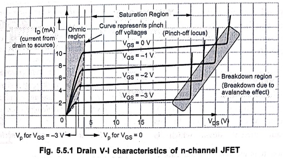
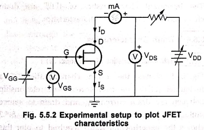
Fig. 5.5.1 shows the drain characteristics of a n‒channel JFET. The curves
represent relationship between the drain current ID and drain to
source voltage VDS for different values of VGS. Fig.
5.5.2 shows the experimental setup required to plot this characteristics.
•
VGS and VDS both =
0: When VGS = 0 the channel is entirely open. But VDS
= 0, so there is no attractive force for the majority carriers (electrons in n‒channel
JFET) and hence drain current does not flow.
• Self pinch‒off at no bias (VGS = 0): At VGS = 0, in response to a small applied voltage VDS, the n‒type bar acts as a simple semiconductor resistor, and the current ID increases linearly with VDS. As VDS increases, the voltage drop along the channel also increases. This increase in voltage drop increases the reverse bias on gate‒source junction and causes the depletion regions to penetrate into the channel, reducing channel width. The effect of reduction in channel width provides more opposition to increase in drain current ID. Thus, rate of increase in ID with respect to VDS is now reduced. This is shown by the curved shape in the characteristics.
•
At some value of VDS, drain current ID cannot be
increased further, due to reduction in channel width. Any further increase in VDS
does not increase the drain current ID. ID approaches the
constant saturation value. The voltage VDS at which the current ID
reaches to its constant saturation level is called 'Pinch‒Off Voltage', VP.
•
VGS with negative bias:
When an external bias, of say ‒1 V, is applied between the gate and the source,
the gate channel junctions are further reverse biased, reducing the effective
width of the channel available for the conduction. Because of this, drain
current will reduce and pinch off voltage is reached at a lower drain current
than when VGS = 0, as shown in Fig. 5.5.1.
•
By applying several values of negative external bias voltage (VGS),
a family of curves are obtained as shown in Fig. 5.5.1. From Fig. 5.5.1 it can
be observed that for more negative values of VGS, the pinch‒off
voltage is reached at lesser values of ID.
•
Breakdown region: We can observe
from Fig. 5.5.1 that if we increase value of VDS beyond pinch‒off
voltage, Vp, the drain current ID remains constant, up to certain
value of VDS. If we further exceed VDS, the voltage will
be reached at which the gate‒channel junction breaks down, due to avalanche
effect. At this point the drain current increases very rapidly, and the device
may be destroyed.
•
It can be observed that the values of VDS for breakdown are reduced
as the negative gate bias is increased. This is because the total reverse breakdown voltage is the
addition of the reverse voltage due to self pinch‒off and the externally
applied voltage VGS.
•
Ohmic and saturation regions:
It
is seen that the drain characteristics of JFET is divided into two regions
ohmic region and saturation region. In the ohmic region, the drain current ID
varies with VDS and the JFET is said to behave as voltage variable
resistance.
In
the saturation region, the drain current ID remains fairly constant
and does not vary with VDS.
•
Cut‒off: As we know, for an n‒channel
JFET, the more negative VGS causes drain current to reduce and pinch‒off
voltage to reach at a lower drain current. When VGS is made
sufficiently negative, ID is reduced to 0, as shown in Fig. 5.5.1.
This is caused by the widening of the depletion region to a point where it
completely closes the channel. The value of VGS at the cut‒off point
is designated as VGS(OFF).
•
Relation of VGS(off) and VP:
ID is 0 when VGS = ‒ VP
Drain Characteristics of p‒Channel JFET
•
In a p‒channel JFET the source is positive with respect to the drain. Here the
source is the source of holes which flow through the channel to the drain. The
pinch‒off is achieved by making the source to gate voltage, VSG
negative (i.e. VGS positive) there by reverse biasing the p‒n
junction diode formed by the channel and the gate.
•
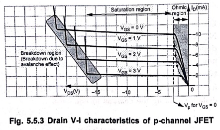
Fig. 5.5.3 shows the drain characteristics of p‒channel JFET. Note the
similarities between these characteristics and those shown for n‒channel JFET
in Fig. 5.5.1.
•
The curves are identical except that voltage VGS and VDS
have reversed polarities and current ID flows in reverse direction.
2. Transfer Characteristics
Transfer Characteristics of n‒Channel JFET
•
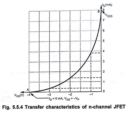
The relationship between the drain current ID and gate to source
voltage V GS is non‒linear
as shown in Fig. 5.5.4. This relationship is defined by Shockley's equation
ID
= IDSS ( 1 ‒ VGS/VP )2
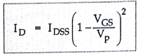
………….. (5.5.1)
•
The squared term of the equation will result in a non‒linear relationship
between ID and VGS producing a curve that grows
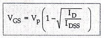
exponentially with decreasing magnitudes of VGS. From equation we
can also write,
•
In the equation values of IDSS and VP are constants,
value of VGD controls ID.
•
A point A at the bottom end of the curve on the VGS‒axis represents
VGS(off), and point B at the top end of the curve on the ID
axis represents IDSS (maximum drain current at VGS =0).
Thus, this curve shows the operating limits of a JFET. These are :
•
ID = 0 when VGS = VGS (off)
•
ID = IDSS when VGS = 0
Transfer Characteristics of p‒Channel JFET
•
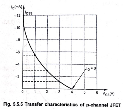
Fig. 5.5.5 shows the transfer characteristics of p‒channel JFET. It is
identical to transfer characteristics of n‒channel JFET except that the
polarities of VGS and ID are reversed.
Review Questions
1. Sketch and explain the drain characteristics for an n‒channel
FET.
2. Draw a circuit diagram to obtain the drain characteristics
for an n‒channel JFET. Thus draw drain characteristics and explain them.
3. Explain the drain characteristics for p‒channel FET.
4. Explain the transfer characteristics for n‒channel JFET.
5. Explain the transfer characteristics for p‒channel JFET.
6. What do you understand by 'pinch off voltages' and 'cut‒off
voltages'?
7. Draw a circuit for obtaining drain and transfer
characteristics for an n‒channel JFET.
8. Sketch a typical drain characteristic for an n‒channel JFET.
Explain the shape of the characteristic and identify the regions.
9. Sketch the basic circuits for both N channel JFET and P‒channel
JFET.
10. Sketch and explain the drain‒characteristics and transfer‒characteristics
of P‒channel JFET.
11. When a FET acts as a voltage variable resistor?
12. Explain the four distinct regions of the output
characteristics of the JFET.
13. Discuss the drain and transfer characteristics of JFETS.
Electron Devices: Chapter 5: Field Effect Transistors : Tag: electronics : - Characteristics of JFET
Electron Devices: Chapter 5: Field Effect Transistors
Under Subject

Electron Devices
EC25C01 2nd Semester ECE Dept | 2025 Regulation | 2nd Semester 2025 Regulation
Related Subjects

English Essentials II
EN25C02 2nd Semester | 2025 Regulation | 2nd Semester 2025 Regulation

Tamils and Technology தமிழர்களும் தொழில்நுட்பமும்
UC25H02 2nd Semester | 2025 Regulation | 2nd Semester 2025 Regulation

Linear Algebra
MA25C02 2nd Semester | 2025 Regulation
Electron Devices
EC25C01 2nd Semester ECE Dept | 2025 Regulation | 2nd Semester 2025 Regulation

Data Structures using CPlusPlus
CS25C05 2nd Semester ECE Dept | 2025 Regulation | 2nd Semester 2025 Regulation

Circuits and Network Analysis
EC25C02 2nd Semester ECE Dept | 2025 Regulation | 2nd Semester 2025 Regulation

Re-Engineering for Innovation
ME25C05 2nd Semester | 2025 Regulation | 2nd Semester 2025 Regulation

Engineering Drawing - Laboratory
ME25C01 2nd Semester | 2025 Regulation | 2nd Semester 2025 Regulation

Data Structures using CPlusPlus - Laboratory
CS25C05 2nd Semester ECE Dept | 2025 Regulation | 2nd Semester 2025 Regulation

Devices and Circuits Laboratory
EC25C03 2nd Semester ECE Dept | 2025 Regulation | 2nd Semester 2025 Regulation