Electron Devices: Chapter 5: Field Effect Transistors
Field Effect Transistors: Two Marks Important Questions and Answers
Electron Devices
Electron Devices: Chapter 5: Field Effect Transistors: Anna University Part A Two Marks Important Questions and Answers
Electron
Devices
Chapter 5: Field Effect
Transistors
Two Marks
Questions with Answers
1. Why is FET called a
unipolar device?
We know that in BJT, the current is carried by both electrons and holes, and hence the name "bipolar" junction transistor. However in FET, current is carried by only one type of charge particles, either electrons or holes. Hence FET is called unipolar device.
2. How can a FET be used as
a voltage controlled resistor?
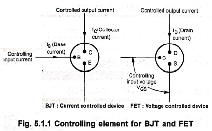
As shown in Fig. 5.1.1, in BJT the output current, IC is controlled by the base current IB. Hence BJT is a current controlled device. On the other hand, in FET, the voltage applied between gate and source (VGS) controls the drain current ID. Therefore, FET is a voltage controlled device.
3. What are the advantages
of FETS?
• Like BJT, the parameters of FET are also temperature dependent. In FET, as temperature increases drain resistance also increases, reducing the drain current. Thus unlike BJT, thermal runaway does not occur with FET. Thus we can say that FET is more temperature stable as compared to the BJT.
• FET has very high input impedance. Typically, it is in the range of one to several megaohms. Because FETs have higher input impedance than BJT they are preferred in amplifiers where high input impedance is required.
• FETs require less space than that for BJTs, hence they are preferred in integrated circuits.
4. Define Amplification
factor in JFET.
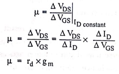
The amplification factor, denoted by μ is defined as,
Amplification factor μ =
μ = rd ×gm
5. Mention the operating
modes of MOSFET.
1.
Depletion mode 2. Enhancement mode.
6. Calculate the
amplification factor, μ of FET, if rd = 4 kΩ and gm = 4
mA/V.
μ = gm rd = 4 × 10‒3
× 4 × 103 = 16
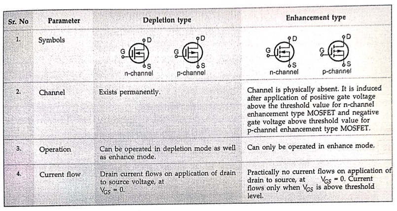
7. Give any two differences
between E‒MOSFET and D‒MOSFET.
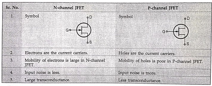
8. Compare p‒channel and n‒channel
JFET.
9. Mention the three
regions that are present in the drain‒source characteristics of JFET.
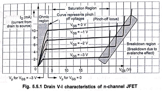
• Self pinch‒off at no bias (VGS = 0): At VGS = 0, in response to a small applied voltage VDS, the n‒type bar acts as a simple semiconductor resistor, and the current ID increases linearly with VDS.
• Breakdown region: We can observe from Fig. 5.5.1 that if we increase value of VDS beyond pinch‒off voltage, Vp, the drain current ID remains constant, up to certain value of VDS.
• Ohmic and saturation regions:
It is seen that the drain characteristics of JFET is divided into two regions ohmic region and saturation region. In the ohmic region, the drain current ID varies with VDS and the JFET is said to behave as voltage variable resistance.
• Cut‒off: As we know, for an n‒channel JFET, the more negative VGS causes drain current to reduce and pinch‒off voltage to reach at a lower drain current.
10. What is pinch‒off
voltage in FET ?
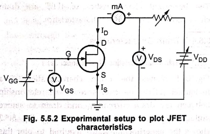
At some value of VDS, drain current ID cannot be increased further, due to reduction in channel width. Any further increase in VDS does not increase the drain current ID. ID approaches the constant saturation value. The voltage VDS at which the current ID reaches to its constant saturation level is called 'Pinch‒Off Voltage', VP.
11. List the
characteristics of JFET.
The important characteristics parameters of JFET are as follows:
• Transconductance (gm)
• Input resistance and capacitance
• Drain to source resistance (rd)
• Amplification factor (μ)
• Power Dissipation (PD).
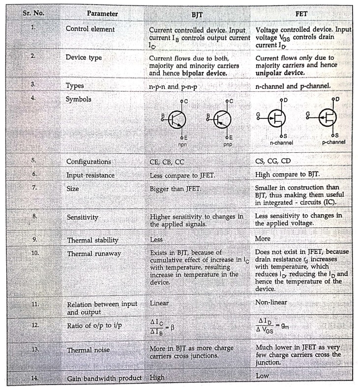
12. Distinguish between BJT
and FET.
13. Give the drain current
equation of JFET
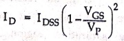
In a transfer characteristics we have seen that the relationship between the drain current ID and gate to source voltage VGS is non‒linear. This relationship is defined by Shockley's equation
14. List the JFET
parameters.
The important characteristics parameters of JFET are as follows:
• Transconductance (gm)
• Input resistance and capacitance
• Drain to source resistance (rd)
• Amplification factor (μ)
• Power Dissipation (PD).
15. List the special
features of FET.
• Voltage Controlled Device: As shown in Fig. 5.1.1, in BJT the output current, IC is controlled by the base current IB. Hence BJT is a current controlled device. On the other hand, in FET, the voltage applied between gate and source (VGS) controls the drain current ID. Therefore, FET is a voltage controlled device.
• The name field effect is derived from the fact that the output current flow is controlled by an electric field set up in the device by an externally applied voltage between gate and source terminals.
• Unipolar Device: We know that in BJT, the current is carried by both electrons and holes, and hence the name "bipolar" junction transistor. However in FET, current is carried by only one type of charge particles, either electrons or holes. Hence FET is called unipolar device.
• Like BJT, the parameters of FET are also temperature dependent. In FET, as temperature increases drain resistance also increases, reducing the drain current. Thus unlike BJT, thermal runaway does not occur with FET. Thus we can say that FET is more temperature stable as compared to the BJT.
• FET has very high input impedance. Typically, it is in the range of one to several megaohms. Because FETs have higher input impedance than BJT they are preferred in amplifiers where high input impedance is required.
• FETs require less space than that for BJTs, hence they are preferred in integrated circuits.
16. In which region JFET
acts as a resistor and why?
In
the ohmic region JFET acts as a resistor as the drain current ID
varies with VDS.
17. Differentiate between
JFET and BJT.
18. Give the current
voltage relationship of the D‒MOSFET and E‒MOSFET.
For
D‒MOSFET,
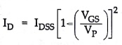
For
E‒MOSFET,
ID
= K[VGS ‒ VT]2
19. What is pinch off
voltage ?
At some value of VDS, drain current ID cannot be increased further, due to reduction in channel width. Any further increase in VDS does not increase the drain current ID. ID approaches the constant saturation value. The voltage VDS at which the current ID reaches to its constant saturation level is called 'Pinch‒Off Voltage', VP.
20. State the application
and difference between BJT and FET.
21. What is a MOS capacitor
?
A
MOS capacitor is a structure consisting of a Metal gate, Oxide layer
(insulator), and Semiconductor substrate. The capacitance of the MOS structure
varies with the applied gate voltage due to the formation of accumulation,
depletion, or inversion layers in the semiconductor.
22. What is nMOS?
In
nMOS technology, electrons are the charge carriers. The transistor conducts
when a positive voltage is applied to the gate terminal, forming a conductive n‒channel
between the source and drain.
23. State two advantages of
nMOS.
1.
Faster operation because electron mobility is high.
2.
Requires smaller chip area for the same current drive.
24. State two disadvantages
of nMOS.
1.
High static power consumption during logic '1'.
2.
Poor noise margin compared to CMOS.
25. What is pMOS ?
In
PMOS technology, conduction occurs through holes. The transistor conducts when
a negative voltage is applied to the gate terminal, forming a p‒channel.
26. State two advantages of
pMOS.
1.
Simple to design and fabricate.
2.
Lower leakage current compared to nMOS.
27. State two disadvantages
of pMOS.
1.
Slower operation due to lower hole mobility.
2.
Requires larger area and higher (negative) voltage.
28. What is CMOS
technology?
CMOS
uses both nMOS and pMOS transistors on the same chip. When one is ON, the other
is OFF, resulting in very low power consumption.
29. State two advantages of
CMOS.
1.
Very low power consumption.
2.
High noise immunity and stable operation.
30. State two disadvantages
of CMOS.
1.
Fabrication is more complex.
2.
May suffer from latch‒up if not designed properly.
Electron Devices: Chapter 5: Field Effect Transistors : Tag: electronics : Electron Devices - Field Effect Transistors: Two Marks Important Questions and Answers
Electron Devices: Chapter 5: Field Effect Transistors
Under Subject

Electron Devices
EC25C01 2nd Semester ECE Dept | 2025 Regulation | 2nd Semester 2025 Regulation
Related Subjects

English Essentials II
EN25C02 2nd Semester | 2025 Regulation | 2nd Semester 2025 Regulation

Tamils and Technology தமிழர்களும் தொழில்நுட்பமும்
UC25H02 2nd Semester | 2025 Regulation | 2nd Semester 2025 Regulation

Linear Algebra
MA25C02 2nd Semester | 2025 Regulation
Electron Devices
EC25C01 2nd Semester ECE Dept | 2025 Regulation | 2nd Semester 2025 Regulation

Data Structures using CPlusPlus
CS25C05 2nd Semester ECE Dept | 2025 Regulation | 2nd Semester 2025 Regulation

Circuits and Network Analysis
EC25C02 2nd Semester ECE Dept | 2025 Regulation | 2nd Semester 2025 Regulation

Re-Engineering for Innovation
ME25C05 2nd Semester | 2025 Regulation | 2nd Semester 2025 Regulation

Engineering Drawing - Laboratory
ME25C01 2nd Semester | 2025 Regulation | 2nd Semester 2025 Regulation

Data Structures using CPlusPlus - Laboratory
CS25C05 2nd Semester ECE Dept | 2025 Regulation | 2nd Semester 2025 Regulation

Devices and Circuits Laboratory
EC25C03 2nd Semester ECE Dept | 2025 Regulation | 2nd Semester 2025 Regulation