Electron Devices: Chapter 5: Field Effect Transistors
Operation of p-Channel and n-Channel JFET
Questions: 1. Explain the operation of n‒channel FET. 2. Sketch a block diagram to represent an n‒channel FET. Indicate voltage and current direction and the device operation. 3. Explain JFET as voltage controlled current source. 4. Explain the working of p‒channel FET. 5. With neat diagram explain the construction, working principle of p‒channel JFET. 6. Illustrate the working mechanism of JFET with necessary diagram.
Operation
of p‒Channel and n‒Channel JFET
Operation of n‒Channel JFET
•
In JFET, the p‒n junction between gate and source is always kept in reverse
biased conditions. Since the current in a reverse biased p‒n junction is
extremely small, practically zero; the gate current in JFET is often neglected
and assumed to be zero.
•
Let us consider the circuit shown in Fig. 5.4.1. As shown in Fig. 5.4.1,
voltage VDD is applied between drain and source. Gate terminal is
kept open. The bar is of n‒type material.
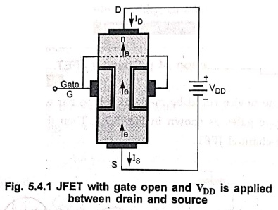
Fig. 5.4.1 JFET with
gate open and VDD is applied between drain and source
•
Due to the applied voltage, the majority carriers i.e. the electrons start
flowing from the source to the drain. This flow of electrons makes the drain
current, ID.
•
The majority carriers (electrons in n‒channel JFET and holes in p‒channel JFET)
move from source to drain through the space between the gate regions. This
space is commonly known as channel. The width of this channel can be controlled
by varying the gate voltage.
•
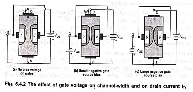
Fig. 5.4.2 (a) shows that an n‒channel JFET with the gate directly connected to
the source terminal. When drain voltage VDS is applied, a drain
current ID flows in the direction shown. Since the n‒material is
resistive, the drain current causes a voltage drop along the channel. This
voltage drop reverse biases the pn junctions, and causes the depletion regions
to penetrate into the channel. Since gate is heavily doped and the channel is
lightly doped, the width of the depletion region will mainly be spread in the
channel shown in Fig. 5.4.2 (a). This penetration depends on the reverse bias
voltage.
•
The depletion region width is more at the drain side as compared to source side
because near the junction, voltage at drain side is more than the voltage at
the source side. This shows that reverse bias is not uniform near the junction;
it gradually increases from source side to drain side.
•
The depletion region does not contain charge carriers, the space between two
depletion regions is available for the conducting portion of the channel. If we
externally apply reverse bias voltage to the gate, the reverse bias will
further increase and hence increase the penetration of the depletion region,
which reduces the width of the conducting portion of the channel. As width of
the conducting portion of the channel reduces, the number of electrons flowing
from source to drain reduces and hence the current flowing from drain to source
reduces.
• If we go on increasing the reverse bias voltage to the gate as shown in Fig. 5.4.2 (b) and 5.4.2 (c), depletion regions will increase more and more and stage will come when the width of the depletion regions will be equal to the original width of the channel, leaving zero width for conducting portion of the channel. This will prevent any current flow from drain to source and hence cut off the drain current. The gate to source voltage that produces cut‒off is known as cut‒off voltage and it is denoted by VGS (off).
•
When the gate is shorted to source, there is minimum reverse bias between gate
and source p‒n junction, making depletion region width minimum and conducting
channel width maximum. In this case maximum drain current flows which is designated
by IDSS.
•
From above discussion it is cleared that the gate to source voltage controls
the current flowing through channel and hence FET is also called voltage
controlled current source.
Operation of p‒Channel JFET
•
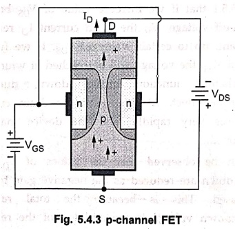
The p‒channel JFET is constructed in exactly the same manner as the n‒channel
JFET but with reversal of the p‒and n‒type materials as shown in Fig. 5.4.3.
•
All current directions and voltage polarities are reversed.
•
For VGS = 0, channel width is maximum. By increasing positive gate
to source (VGS) voltage, the channel width is reduced.
Review Questions
1. Explain the operation of n‒channel FET.
2. Sketch a block diagram to represent an n‒channel FET.
Indicate voltage and current direction and the device operation.
3. Explain JFET as voltage controlled current source.
4. Explain the working of p‒channel FET.
5. With neat diagram explain the construction, working principle
of p‒channel JFET.
6. Illustrate the working mechanism of JFET with necessary
diagram.
Electron Devices: Chapter 5: Field Effect Transistors : Tag: electronics : - Operation of p-Channel and n-Channel JFET
Electron Devices: Chapter 5: Field Effect Transistors
Under Subject

Electron Devices
EC25C01 2nd Semester ECE Dept | 2025 Regulation | 2nd Semester 2025 Regulation
Related Subjects

English Essentials II
EN25C02 2nd Semester | 2025 Regulation | 2nd Semester 2025 Regulation

Tamils and Technology தமிழர்களும் தொழில்நுட்பமும்
UC25H02 2nd Semester | 2025 Regulation | 2nd Semester 2025 Regulation

Linear Algebra
MA25C02 2nd Semester | 2025 Regulation
Electron Devices
EC25C01 2nd Semester ECE Dept | 2025 Regulation | 2nd Semester 2025 Regulation

Data Structures using CPlusPlus
CS25C05 2nd Semester ECE Dept | 2025 Regulation | 2nd Semester 2025 Regulation

Circuits and Network Analysis
EC25C02 2nd Semester ECE Dept | 2025 Regulation | 2nd Semester 2025 Regulation

Re-Engineering for Innovation
ME25C05 2nd Semester | 2025 Regulation | 2nd Semester 2025 Regulation

Engineering Drawing - Laboratory
ME25C01 2nd Semester | 2025 Regulation | 2nd Semester 2025 Regulation

Data Structures using CPlusPlus - Laboratory
CS25C05 2nd Semester ECE Dept | 2025 Regulation | 2nd Semester 2025 Regulation

Devices and Circuits Laboratory
EC25C03 2nd Semester ECE Dept | 2025 Regulation | 2nd Semester 2025 Regulation