Electron Devices: Chapter 5: Field Effect Transistors
Depletion MOSFET (D-MOSFET)
Construction, Operation, Characteristics, Parameters, Type, Symbols

Questions: 1. Explain the construction, operation and characteristics of n‒channel depletion type MOSFET. 2. Define transconductance. 3. With the help of suitable diagrams explain the working of different types of MOSFET. 4. Sketch the graph symbol for n ‒ channel and p channel MOSFET. 5. Discuss your understanding on MOSFET detailing the types, construction and characteristics. 6. Describe the output and transfer characteristics of MOSFET.
Depletion
MOSFET (D‒MOSFET)
1. Construction of n‒channel MOSFET
•
Fig. 5.12.1 shows the basic construction of n‒channel depletion type MOSFET.
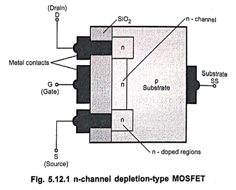
Fig. 5.12.1 n‒channel depletion‒type MOSFET
•
Two highly doped n‒regions are diffused into a lightly doped p‒type substrate.
•
These two highly doped n‒regions represent source and drain. Usually substrate
is internally connected to the source terminal.
•
The source and drain terminals are connected through metallic contacts to n‒doped
regions linked by an n‒channel as shown in Fig. 5.12.1.
•
The gate is also connected to a metal contact surface but remains insulated
from the n‒channel by a very thin layer of dielectric material, silicon dioxide
(SiO2).
•
Thus, there is no direct electrical connection between the gate terminal and
the channel of a MOSFET, increasing the input impedance of the device.
2. Operation, Characteristics and Parameters of n‒channel MOSFET
•
On the application of drain to source voltage, VDS and keeping gate
to source voltage to zero by directly connecting gate terminal to the source
terminal, free electrons from the n‒channel are attracted towards positive
potential of drain terminal.
•
This establishes current through the channel to be denoted as IDSS
at VGS = 0 V, as shown in Fig. 5.12.2.
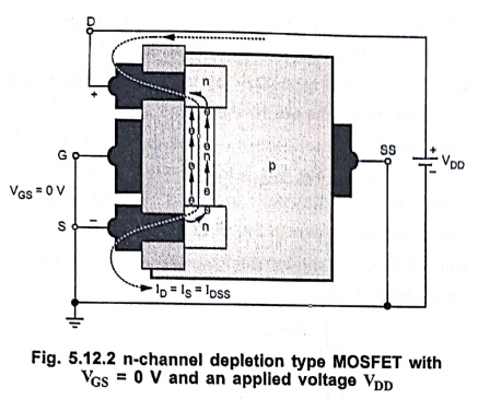
Fig. 5.12.2 n‒channel
depletion type MOSFET with VGS= 0 V and an applied voltage VDD
•
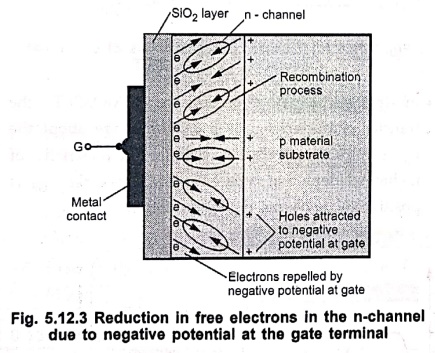
If we apply negative gate voltage, the negative charges on the gate repel
conduction electrons from the channel, and attract holes from the p‒type
substrate.
•
This initiates recombination of repelled electrons and attracted holes as shown
in Fig. 5.12.3.
•
The level of recombination between electrons and holes depends on the magnitude
of the negative voltage applied at the gate.
•
This recombination reduces the number of free electrons in the n‒channel for
the conduction, reducing the drain current.
•
In other words we can say that, due to recombinations, n‒channel is depleted of
some of its electrons, thus decreasing the channel conductivity.
•
The greater the negative voltage applied at the gate, the greater the depletion
of n‒channel electrons.
•
The level of drain current will reduce with increasing negative bias for VGS
as shown in the transfer characteristics of depletion type MOSFET (Fig.
5.12.4).
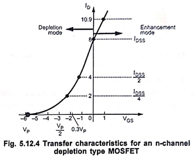
Fig. 5.12.4 Transfer
characteristics for an n‒channel depletion type MOSFET
•
For positive values of VGS the positive gate will draw additional
electrons from the p‒type substrate due to reverse leakage current and
establish new carriers through the collisions between accelerating particles.
Because of this, as gate to source voltage increases in positive direction, the
drain current also increases as shown in Fig. 5.12.4.
•
The application of a positive gate to source voltage has "enhanced"
the level of free carriers in the channel compared to that encountered with VGS
= 0 V. For this reason the region of positive gate voltages on the drain or
transfer characteristics is referred to as enhancement region and the region
between cut‒off and the saturation levels of IDSS referred to as
depletion region.
•
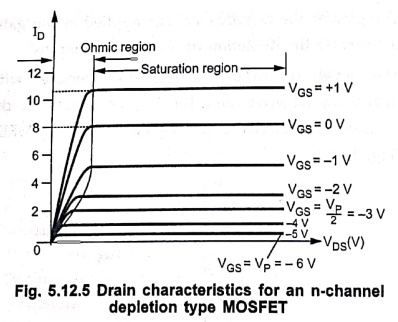
Fig. 5.12.5 shows drain characteristics for n‒channel depletion type MOSFET. It
is similar to that of JFET. The only difference is that it has positive part of
VGS.
Transconductance (gm)
•
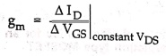
It is defined as the ratio of change in drain current to the corresponding
change in gate to source voltage, at a constant of drain to source voltage
Important Concept
1.
ID = 0 corresponds to VGS(off), VGS(off) = − VP.
2.
VGS = 0 corresponds to IDSS.
3.
Both positive and negative values of VGS can be used to bias D‒MOSFET.
3. p‒Channel Depletion Type MOSFET
• The construction of the p‒channel depletion type MOSFET is exactly opposite of that of n‒channel depletion type MOSFET.
•
Here, the substrate is of n‒type, and regions and channels are of p‒type as
shown in Fig. 5.12.6 (a).
•
As shown in Fig. 5.12.6 (a) voltage polarities and current directions are
reversed.
•
The drain characteristics appear exactly as in Fig. 5.12.6 (b) but VDS
with negative values, ID in the opposite direction and VGS
having opposite polarities as shown in Fig. 5.12.6 (b).
•
Fig. 5.12.6 (c) shows the transfer characteristics of p‒channel depletion type
MOSFET.
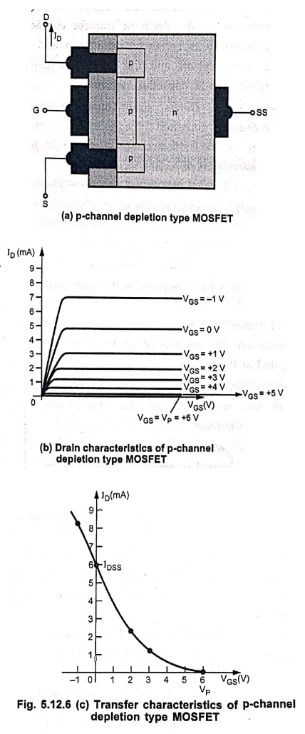
• In the p‒channel depletion type MOSFET, the transfer characteristics is a mirror image about the ID axis (Y axis) of the transfer characteristic of n‒channel depletion type MOSFET, since the VGS is positive in p‒channel depletion region.
4. D‒MOSFET Symbols
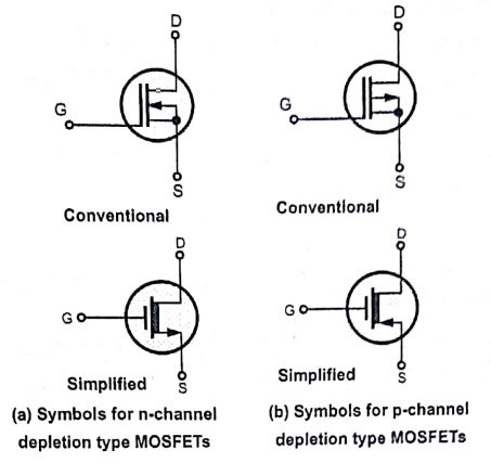
Fig.
5.12.7 shows graphic symbols for a n and p‒channel depletion type MOSFET.
Review
Questions
1. Explain the construction, operation and characteristics of n‒channel
depletion type MOSFET.
2. Define transconductance.
3. With the help of suitable diagrams explain the working of
different types of MOSFET.
4. Sketch the graph symbol for n ‒ channel and p channel MOSFET.
5. Discuss your understanding on MOSFET detailing the types,
construction and characteristics.
6. Describe the output and transfer characteristics of MOSFET.
Electron Devices: Chapter 5: Field Effect Transistors : Tag: electronics : Construction, Operation, Characteristics, Parameters, Type, Symbols - Depletion MOSFET (D-MOSFET)
Electron Devices: Chapter 5: Field Effect Transistors
Under Subject

Electron Devices
EC25C01 2nd Semester ECE Dept | 2025 Regulation | 2nd Semester 2025 Regulation
Related Subjects

English Essentials II
EN25C02 2nd Semester | 2025 Regulation | 2nd Semester 2025 Regulation

Tamils and Technology தமிழர்களும் தொழில்நுட்பமும்
UC25H02 2nd Semester | 2025 Regulation | 2nd Semester 2025 Regulation

Linear Algebra
MA25C02 2nd Semester | 2025 Regulation
Electron Devices
EC25C01 2nd Semester ECE Dept | 2025 Regulation | 2nd Semester 2025 Regulation

Data Structures using CPlusPlus
CS25C05 2nd Semester ECE Dept | 2025 Regulation | 2nd Semester 2025 Regulation

Circuits and Network Analysis
EC25C02 2nd Semester ECE Dept | 2025 Regulation | 2nd Semester 2025 Regulation

Re-Engineering for Innovation
ME25C05 2nd Semester | 2025 Regulation | 2nd Semester 2025 Regulation

Engineering Drawing - Laboratory
ME25C01 2nd Semester | 2025 Regulation | 2nd Semester 2025 Regulation

Data Structures using CPlusPlus - Laboratory
CS25C05 2nd Semester ECE Dept | 2025 Regulation | 2nd Semester 2025 Regulation

Devices and Circuits Laboratory
EC25C03 2nd Semester ECE Dept | 2025 Regulation | 2nd Semester 2025 Regulation