Electron Devices: Chapter 5: Field Effect Transistors
Characteristics Parameters of JFET
Questions: 1. Sketch a typical transfer characteristic for an n‒channel JFET and show how the transconductance gm can be derived from the transfer characteristic. 2. Define the following parameters of JFET : 1) Transconductance 2) Drain resistance 3) Amplification factor 4) Power dissipation.
Characteristics
Parameters of JFET
The
important characteristics parameters of JFET are as follows:
•
Transconductance (gm)
•
Input resistance and capacitance
•
Drain to source resistance (rd)
•
Amplification factor (μ)
•
Power Dissipation (PD).
• Transconductance
•
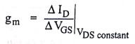
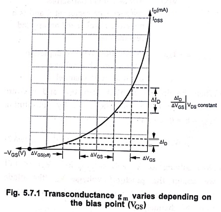
The transconductance, gm, is the change in the drain current for
given change in gate to source voltage with the drain to source voltage
constant as shown in Fig. 5.7.1.
•
Looking at Fig. 5.7.1, we can say that it is the slope of the transfer
characteristic. Since the slope varies, gm also varies. gm
has a greater value near the top of the curve than it does near the bottom. The
transconductance gm is defined as
•
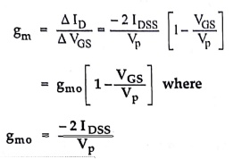
The transconductance gm is also called mutual conductance. The
practical unit for gm is mS (millisiemen) or mA/V. For given gm,
we can calculate an approximate value for gm at any point on the
transfer characteristic curve using following equation.
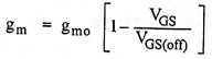
………... (5.7.2)
•
where gmo is the value of gm
for VGS = 0, and is given by,
gmo = ‒2IDSS / VP
………. (5.7.3)
•
This can be proved as given below. We know that,
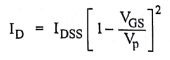
•
Differentiating this equation with respect to VGS we get,
Ex. 5.7.1: For JFET, if IDSS = 20
mA, VGS(off) = − 5 V, and gmo = 4 mS or mA/V. Determine
the transconductance for VGS = ‒ 4 V, and find ID at this
point.
Solution:
From
equation (5.7.2) we have,

= 4×10‒3 × 0.2 = 0.8 mS
We
have,

= 20×10‒3 × 0.04 = 0.8 mA
• Input Resistance and Capacitance
•
We know that a JFET operates with its gate source junction reverse‒biased.
Therefore, the input resistance at the gate is very high. This high input
resistance is one advantage of the JFET over the bipolar transistor. (Recall
that a BJT operates with a forward biased base‒emitter junction). JFET data
sheets often specify the input resistance by giving a value of the gate reverse
current, IGSS at a certain gate to source voltage, VGS. The
input resistance can then be determined using the following equation, where the
vertical lines indicate an absolute value.
RIN
= | VGS / IGSS |
•
For example, the 2N3909 data sheet lists a maximum IGSS of 10 nA for
VGS = 10 V at 25 °C. Therefore,
RIN
= | 10V / 10nA | = 1000 ΜΩ
•
From data sheet we can also observe that IGSS is 1.0 μA for VGS = 10
V at 100 °C. This shows that IGSS increases with temperature. Here,
RIN = | 10V / 1μΑ | = 10 ΜΩ
Key
Point: The input resistance decreases with increase in
temperature.
•
The input capacitance, Ciss is a result of the JFET operating with a
reverse biased p‒n junction. Recall that a reverse biased p‒n junction acts as
a capacitor whose capacitance depends on the amount of reverse voltage. For
example, the 2N3909 has a maximum Ciss of 32 pF for VGS =
0.
• Drain to Source Resistance
•
From the drain characteristic, the important parameter of JFET, drain
resistance rd, can be calculated. Fig. 5.7.2 shows the drain
characteristics of n‒channel JFET.
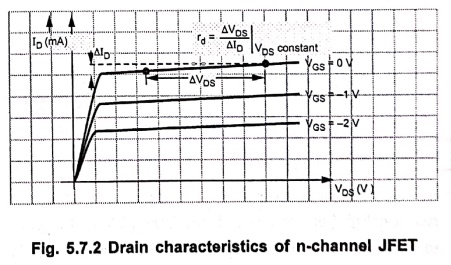
Fig. 5.7.2 Drain characteristics of n‒channel
JFET
•
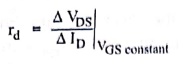
The drain resistance rd is the a.c. resistance between drain and
source terminals when the JFET is operating in the saturation region. It is the
reciprocal of the slope of the drain characteristic in the saturation region.
It is given by,
•
Since the characteristics in the saturation region is almost flat, rd
is not easily determined from the characteristics. Values of rd
range from about 50 kΩ to several 100 kΩ. Since rd is usually the
output resistance of the JFET, it may also be expressed as an output admittance
|Yos| = 1/rd.
• Amplification Factor
•
The amplification factor, denoted by μ is defined as,
Amplification factor μ =
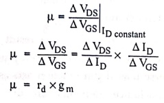
μ = rd ×gm
…………. (5.7.5)
• Power Dissipation (PD)
•
The power dissipation in JFET is given by,
PD = ID × VDS
Review Questions
1. Sketch a typical transfer characteristic for an n‒channel
JFET and show how the transconductance gm can be derived from the transfer
characteristic.
2. Define the following parameters of JFET :
1) Transconductance
2) Drain resistance
3) Amplification factor
4) Power dissipation.
Electron Devices: Chapter 5: Field Effect Transistors : Tag: electronics : - Characteristics Parameters of JFET
Electron Devices: Chapter 5: Field Effect Transistors
Under Subject

Electron Devices
EC25C01 2nd Semester ECE Dept | 2025 Regulation | 2nd Semester 2025 Regulation
Related Subjects

English Essentials II
EN25C02 2nd Semester | 2025 Regulation | 2nd Semester 2025 Regulation

Tamils and Technology தமிழர்களும் தொழில்நுட்பமும்
UC25H02 2nd Semester | 2025 Regulation | 2nd Semester 2025 Regulation

Linear Algebra
MA25C02 2nd Semester | 2025 Regulation
Electron Devices
EC25C01 2nd Semester ECE Dept | 2025 Regulation | 2nd Semester 2025 Regulation

Data Structures using CPlusPlus
CS25C05 2nd Semester ECE Dept | 2025 Regulation | 2nd Semester 2025 Regulation

Circuits and Network Analysis
EC25C02 2nd Semester ECE Dept | 2025 Regulation | 2nd Semester 2025 Regulation

Re-Engineering for Innovation
ME25C05 2nd Semester | 2025 Regulation | 2nd Semester 2025 Regulation

Engineering Drawing - Laboratory
ME25C01 2nd Semester | 2025 Regulation | 2nd Semester 2025 Regulation

Data Structures using CPlusPlus - Laboratory
CS25C05 2nd Semester ECE Dept | 2025 Regulation | 2nd Semester 2025 Regulation

Devices and Circuits Laboratory
EC25C03 2nd Semester ECE Dept | 2025 Regulation | 2nd Semester 2025 Regulation