Electron Devices: Chapter 5: Field Effect Transistors
nMOS and PMOS
Advantages, Disadvantages, Applications, Inverter
Questions: 1. What is n‒MOS and p‒MOS? 2. State advantages and disadvantages of n‒MOS. 3. State advantages and disadvantages of p‒MOS. 4. Explain the nMOS inverter. 5. Explain the pMOS inverter.
nMOS
and PMOS
nMOS (n‒Channel Metal‒Oxide‒Semiconductor)
•
In nMOS technology, the MOSFETS use n‒type carriers (electrons) for conduction.
An nMOS transistor conducts when a positive voltage is applied to the gate
terminal. It offers high switching speed due to the higher mobility of
electrons.
Advantages
•
Faster operation because electron mobility is higher than hole mobility.
•
Requires smaller area for the same drive current.
•
Easier to fabricate compared to pMOS.
Disadvantages
•
High static power consumption due to continuous current flow during logic
"1′′ output.
•
Poor noise margin compared to CMOS.
•
Requires additional circuitry to achieve full logic levels.
Applications
•
Used in early digital ICs, memory cells, and some analog switches.
nMOS Inverter
Fig.
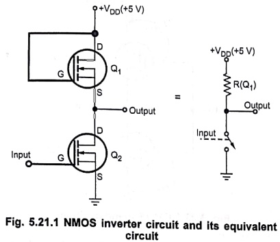
5.21.1 shows the basic NMOS inverter circuit. It contains two N‒channel
MOSFETs. Q2 is a switching MOSFET and Q1 is a load
MOSFET. Q1 acts as load resistance (Rd) for Q2. As gate
of Q1 is permanently connected to the VDD, it is always
ON, and hence the load resistance is equal to the RON of the MOSFET.
Particularly, Q1 is designed to have greater RON than the
RON of Q2. To achieve this channel of Q1 is
made much narrower than channel of Q2. Typically RON of Q1
is 100k whereas RON of Q2 is 1 kΩ. We know that MOS
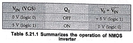
devices are voltage controlled devices. When positive voltage (HIGH input) is
applied between gate and source, Q2 is switched ON and it makes the
output low. On the other hand, when input is LOW Q2 is switched OFF
and therefore, output is high.
PMOS (p‒Channel Metal‒Oxide‒Semiconductor)
•
In PMOS technology, conduction is by holes (p‒type carriers). A pMOS transistor
conducts when a negative voltage is applied to the gate terminal. It was
popular before nMOS became dominant.
Advantages
•
Simple to design and fabricate.
•
Less leakage current compared to nMOS.
•
Good for low‒speed, low‒noise applications.
Disadvantages
•
Slower operation because hole mobility is much lower than electron mobility.
•
Requires higher operating voltage (negative bias).
•
Larger chip area needed for the same current drive as nMOS.
Applications
•
Used in early‒generation logic circuits and analog ICs where speed is not
critical.
pMOS Inverter
Fig.
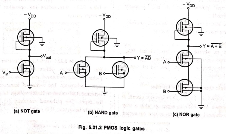
5.21.2 shows PMOS inverter, NAND gate and P‒channel, enhancement‒type NOR gate.
For MOSFET a negative voltage is needed at the gate terminal to form a channel.
According to the positive logic, logic‒0 is approximately ‒ VDD<‒VT
which is the low‒voltage signal value, while logic‒1 is approximately ground,
which is the high voltage signal value.
Review Questions
1. What is n‒MOS and p‒MOS?
2. State advantages and disadvantages of n‒MOS.
3. State advantages and disadvantages of p‒MOS.
4. Explain the nMOS inverter.
5. Explain the pMOS inverter.
Electron Devices: Chapter 5: Field Effect Transistors : Tag: electronics : Advantages, Disadvantages, Applications, Inverter - nMOS and PMOS
Electron Devices: Chapter 5: Field Effect Transistors
Under Subject

Electron Devices
EC25C01 2nd Semester ECE Dept | 2025 Regulation | 2nd Semester 2025 Regulation
Related Subjects

English Essentials II
EN25C02 2nd Semester | 2025 Regulation | 2nd Semester 2025 Regulation

Tamils and Technology தமிழர்களும் தொழில்நுட்பமும்
UC25H02 2nd Semester | 2025 Regulation | 2nd Semester 2025 Regulation

Linear Algebra
MA25C02 2nd Semester | 2025 Regulation
Electron Devices
EC25C01 2nd Semester ECE Dept | 2025 Regulation | 2nd Semester 2025 Regulation

Data Structures using CPlusPlus
CS25C05 2nd Semester ECE Dept | 2025 Regulation | 2nd Semester 2025 Regulation

Circuits and Network Analysis
EC25C02 2nd Semester ECE Dept | 2025 Regulation | 2nd Semester 2025 Regulation

Re-Engineering for Innovation
ME25C05 2nd Semester | 2025 Regulation | 2nd Semester 2025 Regulation

Engineering Drawing - Laboratory
ME25C01 2nd Semester | 2025 Regulation | 2nd Semester 2025 Regulation

Data Structures using CPlusPlus - Laboratory
CS25C05 2nd Semester ECE Dept | 2025 Regulation | 2nd Semester 2025 Regulation

Devices and Circuits Laboratory
EC25C03 2nd Semester ECE Dept | 2025 Regulation | 2nd Semester 2025 Regulation