Electron Devices: Chapter 5: Field Effect Transistors
CMOS
Advantages, Disadvantages, Applications, Basic Operation as an Inverter
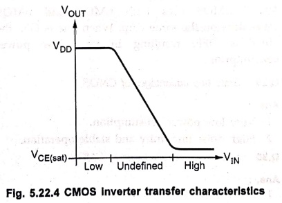
Questions: 1. What is CMOS technology. 2. State advantages and disadvantages of CMOS technology. 3. Explain the CMOS inverter. 4. Sketch the typical transfer characteristics of a CMOS inverter.
CMOS
•
CMOS technology combines nMOS and pMOS transistors on the same chip. When one
transistor (nMOS) is ON, the other (pMOS) is OFF thus minimizing power loss. It
is the most widely used technology in modern ICs.
Advantages
•
Very low power consumption, since only leakage current flows when idle.
•
High noise immunity and stable operation over a wide voltage range.
•
High packing density and excellent scalability for large‒scale integration.
•
Combines the speed of nMOS with the low power of pMOS.
Disadvantages
•
More complex fabrication process compared to nMOS or PMOS alone.
•
Susceptible to latch‒up (a short circuit between power rails if not properly
designed).
•
Static sensitivity ‒ must be handled carefully during manufacturing and
testing.
Applications
•
Used in almost all modern digital ICs, microprocessors, microcontrollers,
memories and low‒power devices like smartphones and laptops.
Basic Operation as an Inverter
Fig.
5.22.1 shows the basic CMOS inverter circuit. It consists of two MOSFETs in
series in such a way that the p‒channel device has its source connected to +VDD
(a positive voltage) and the n‒channel device has its source connected to
ground.
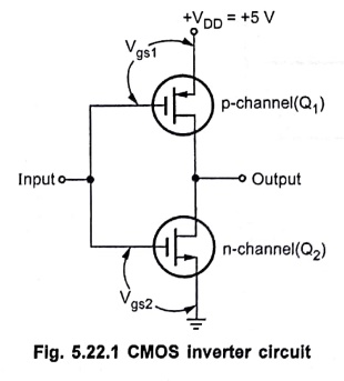
The
gates of the two devices are connected together as the common input and the
drains are connected together as the common output.
1.
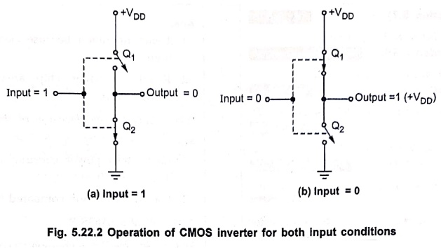
When input is HIGH, the gate of Q1 (p‒channel) is at 0 V relative to
the source of Q1 i.e. Vgs1 =0V. Thus, Q1 is
OFF. On the other hand, the gate of Q2 (n‒channel) is at +VDD
relative to its source i.e. Vgs2 = +VDD. Thus, Q2
is ON. This will produce VOUT ≈ 0 V, as shown in Fig. 5.22.2 (a).
2.
When input is LOW, the gate of Q1 (p‒channel) is at a negative
potential relative to its source while Q2 has Vgs = 0 V.
Thus, Q1 is ON and Q2 is OFF. This produces output
voltage approximately + VDD, as shown in Fig. 5.22.2 (b).
•
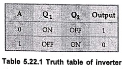
Table 5.22.1 summarizes the operation of CMOS inverter circuit.
•
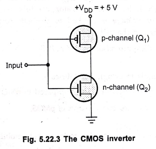
Fig. 5.22.3 shows, different symbols used for the p‒channel and n‒channel
transistors to reflect their logical behaviour. The n‒channel transistor (Q2)
is switched 'ON' when a HIGH voltage is applied at the input. The p‒channel
transistor (Q1) has the opposite behaviour, it is switched ON when a
LOW voltage is applied at the input. It is indicated by placing bubble in the
symbol.
•
Fig. 5.22.4 shows the transfer characteristics of CMOS inverter.
Review
Questions
1. What is CMOS technology.
2. State advantages and disadvantages of CMOS technology.
3. Explain the CMOS inverter.
4. Sketch the typical transfer characteristics of a CMOS
inverter.
Electron Devices: Chapter 5: Field Effect Transistors : Tag: electronics : Advantages, Disadvantages, Applications, Basic Operation as an Inverter - CMOS
Electron Devices: Chapter 5: Field Effect Transistors
Under Subject

Electron Devices
EC25C01 2nd Semester ECE Dept | 2025 Regulation | 2nd Semester 2025 Regulation
Related Subjects

English Essentials II
EN25C02 2nd Semester | 2025 Regulation | 2nd Semester 2025 Regulation

Tamils and Technology தமிழர்களும் தொழில்நுட்பமும்
UC25H02 2nd Semester | 2025 Regulation | 2nd Semester 2025 Regulation

Linear Algebra
MA25C02 2nd Semester | 2025 Regulation
Electron Devices
EC25C01 2nd Semester ECE Dept | 2025 Regulation | 2nd Semester 2025 Regulation

Data Structures using CPlusPlus
CS25C05 2nd Semester ECE Dept | 2025 Regulation | 2nd Semester 2025 Regulation

Circuits and Network Analysis
EC25C02 2nd Semester ECE Dept | 2025 Regulation | 2nd Semester 2025 Regulation

Re-Engineering for Innovation
ME25C05 2nd Semester | 2025 Regulation | 2nd Semester 2025 Regulation

Engineering Drawing - Laboratory
ME25C01 2nd Semester | 2025 Regulation | 2nd Semester 2025 Regulation

Data Structures using CPlusPlus - Laboratory
CS25C05 2nd Semester ECE Dept | 2025 Regulation | 2nd Semester 2025 Regulation

Devices and Circuits Laboratory
EC25C03 2nd Semester ECE Dept | 2025 Regulation | 2nd Semester 2025 Regulation