Electron Devices: Chapter 5: Field Effect Transistors
Field Effect Transistors
Symbol, Features, Classification

Questions: 1. What is FET? 2. What is JFET ? 3. List important features of FET. 4. Give the classification of FET.
Electron Devices
Chapter 5: Field Effect Transistors
Introduction
•
The Field Effect Transistor abbreviated as FET is an another semiconductor
device like a BJT which can be used as an amplifier or switch. Like BJT, FET is
also a three terminal device; however, the principle of operation of FET is
completely different from that of BJT.
•
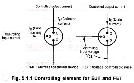
The three terminals of FET are named as Drain (D), Source (S) and Gate (G), as
shown in Fig. 5.1.1. Out of these three terminals gate terminal acts as a
controlling terminal.
Features of FET
• Voltage Controlled
Device: As shown in Fig. 5.1.1, in BJT the output current,
IC is controlled by the base current IB. Hence BJT is a
current controlled device. On the other hand, in FET, the voltage applied
between gate and source (VGS) controls the drain current ID.
Therefore, FET is a voltage controlled device.
• The name field effect is derived from the fact that the output current flow is controlled by an electric field set up in the device by an externally applied voltage between gate and source terminals.
•
Unipolar Device: We know that in
BJT, the current is carried by both electrons and holes, and hence the name
"bipolar" junction transistor. However in FET, current is carried by
only one type of charge particles, either electrons or holes. Hence FET is
called unipolar device.
•
Like BJT, the parameters of FET are also temperature dependent. In FET, as
temperature increases drain resistance also increases, reducing the drain
current. Thus unlike BJT, thermal runaway does not occur with FET. Thus we can
say that FET is more temperature stable as compared to the BJT.
•
FET has very high input impedance. Typically, it is in the range of one to
several megaohms. Because FETs have higher input impedance than BJT they are
preferred in amplifiers where high input impedance is required.
•
FETs require less space than that for BJTs, hence they are preferred in
integrated circuits.
Classification of FET
The
FETs are categorised as :
•
Junction Field Effect Transistors (JFETs),
•
Metal Oxide Semiconductor Field Effect Transistors (MOSFETs)
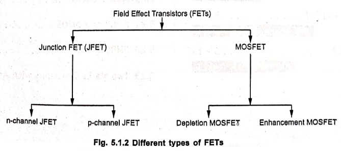
The JFETs are further classified into two types as, n‒channel JFET and p‒channel JFET and MOSFETs are further classified into two types as, depletion MOSFET and enhancement MOSFET. Fig. 5.1.2 shows the different types of FETs.
•
In JFET, there is a direct electrical connection. between the gate terminal and
the channel of a JFET.
•
On the other hand, in MOSFETs, the gate is insulated from the channel by a very
thin layer of dielectric material, silicon dioxide (SiO2). Thus, in
MOSFETs, there is no direct electrical connection between the gate terminal and
the channel. Due to this extra layer the input resistance of MOSFET is very
very high.
Review
Questions
1. What is FET?
2. What is JFET ?
3. List important features of FET.
4. Give the classification of FET.
Electron Devices: Chapter 5: Field Effect Transistors : Tag: electronics : Symbol, Features, Classification - Field Effect Transistors
Electron Devices: Chapter 5: Field Effect Transistors
Under Subject

Electron Devices
EC25C01 2nd Semester ECE Dept | 2025 Regulation | 2nd Semester 2025 Regulation
Related Subjects

English Essentials II
EN25C02 2nd Semester | 2025 Regulation | 2nd Semester 2025 Regulation

Tamils and Technology தமிழர்களும் தொழில்நுட்பமும்
UC25H02 2nd Semester | 2025 Regulation | 2nd Semester 2025 Regulation

Linear Algebra
MA25C02 2nd Semester | 2025 Regulation
Electron Devices
EC25C01 2nd Semester ECE Dept | 2025 Regulation | 2nd Semester 2025 Regulation

Data Structures using CPlusPlus
CS25C05 2nd Semester ECE Dept | 2025 Regulation | 2nd Semester 2025 Regulation

Circuits and Network Analysis
EC25C02 2nd Semester ECE Dept | 2025 Regulation | 2nd Semester 2025 Regulation

Re-Engineering for Innovation
ME25C05 2nd Semester | 2025 Regulation | 2nd Semester 2025 Regulation

Engineering Drawing - Laboratory
ME25C01 2nd Semester | 2025 Regulation | 2nd Semester 2025 Regulation

Data Structures using CPlusPlus - Laboratory
CS25C05 2nd Semester ECE Dept | 2025 Regulation | 2nd Semester 2025 Regulation

Devices and Circuits Laboratory
EC25C03 2nd Semester ECE Dept | 2025 Regulation | 2nd Semester 2025 Regulation