Electron Devices: Chapter 2: PN Junction Diodes
Derivation of V‒I Characteristics of PN Junction Diode (Diode Current Equation)
Let us study the derivation of the mathematical expression for the current through a diode, which gives its V‒I characteristics.
Derivation
of V‒I Characteristics of P‒N Junction Diode (Diode Current Equation)
•
Let us study the derivation of the mathematical expression for the current
through a diode, which gives its V‒I characteristics.
Let
Pp
= Hole concentration in p‒type at the edge of depletion region
nn
= Electron concentration in n‒type at the edge of depletion region
Pn
= Hole concentration in n‒type at the edge of depletion region
np
= Electron concentration in p‒type at the edge of depletion region
Key
Point: Note that in the symbol, basic letter indicates
type of charge carrier concentration hole (p) or electron (n). The base
indicates type of material in which it exists.
•
Under unbiased condition, when holes move from p‒side to n‒side due to
diffusion, their concentration behaves exponentially. This is mathematically
expressed as,
Pp
= Pn eVj/VT
...(2.10.1)
where
VJ = Barrier potential or junction potential
•
Now consider forward biased diode as shown in x = 0.
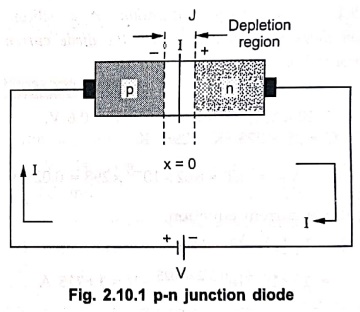
Fig. 2.10.1 p‒n
junction diode
•
Though the proportion of holes and electrons in constituting a current through
the p‒region is changing, the hole concentration throughout the entire p‒region
is constant and denoted as,
Pp0 = Hole concentration in p‒region
•
As holes cross the junction, this, concentration becomes Pn(0) which
is concentration of holes on n‒side just near the junction. This further
behaves exponentially as given in the equation (2.10.1).
•
From equation (2.10.1) we can write,
Pp0 = Pn(0) e(VJ‒V)/.VT
………..(2.10.2)
Key
Point: The term VJ becomes VJ ‒ V as
the forward biased voltage V opposes the barrier potential. So net voltage
across the junction becomes VJ‒V.
•
The equation (2.10.2) can be written for open circuited unbiased p‒n junction
diode by putting V = 0 as,
Pp0
= Pn0 eVJ/VT
….....(2.10.3)
where
Pno is the concentration of holes on n‒side just near the junction
when diode is open circuited i.e. at thermal equilibrium and hence different
than pn(0).
•
As the concentration of holes in entire p‒region is constant, equating
equations (2.10.2) and (2.10.3) we get,
Pn(0)
eVJ‒V/VT
= Pn0 eVJ/VT
Pn(0)
= Pn0 eVJ/VT
...(2.10.4)
•
This equation represents boundary condition and called law of junction. This
indicates that the hole concentration Pn(0) at the junction under
forward biased condition is greater than its thermal equilibrium value Pn0
For large forward biasing Pn(0) becomes much larger compared to Pn0.
Key
Point: The discussion is equally applicable for the
electron concentration on the p‒side.
•
Thus, np(0) = np0 eV/VT
...(2.10.5)
•
Now the difference between two concentrations at the junction under unbiased
and biased condition is called injected or excess concentration denoted as Pn(0).
Pn(0) = Pn(0) ‒ Pn0
...(2.10.6)
•
Using equation (2.10.4) in equation (2.10.6),
Pn(0) = Pn0 eV/VT‒
Pn0
Pn(0) = Pn0 (eV/VT‒
1) ...(2.10.7)
Similarly,
Np(0) = Pp0 (eV/VT‒
1) ...(2.10.8)
•
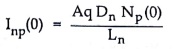
The hole current crossing the junction from p‒side to n‒side is given by,
Ipn (0) = [ Aq Dp Pn (0) ] / Lp
...(2.10.9)
While
an electron current crossing the junction from n‒side to p‒side is given by,
Inp(0) = [ Aq Dn Np(0) ] / Ln
...(2.10.10)
where
A
= Area of cross‒section of junction
DP
= Diffusion constant for holes,
Dn
= Diffusion constant for electrons
Lp
= Diffusion length for holes,
Ln
= Diffusion length for electrons
•
Using equations (2.10.7) and (2.10.8) in equations (2.10.9) and (2.10.10), the
total current I at the junction is given by,
I
= Ipn(0) + Inp(0)
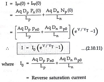
I0
= Reverse saturation current
•
The equation (2.10.11) is the required expression for diode current.
Key
Point: In the derivation, the generation and
recombination in the depletion region is neglected. To consider its effect,
which is dominant in Si diodes, the factor η is introduced in the equation.
I0
= I0 (eV/ηVT
‒1)
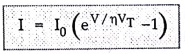
The value of η = 1 for Ge diodes and η = 2 for
Si diodes.
Carrier Lifetimes
•
In a pure semiconductor the number of free electrons is always equal to number
of holes. The thermal agitation continues to produce new hole‒electron pairs
while previous pairs disappear. This disappearing of pairs is due to the
process called recombination. The merging of of a free electron and hole is
called recombination. The amount of time between the creation and disappearence
of a free electron and hole pair is called its lifetime.
•
Thus a hole exists for τр seconds before it recombines while a free
electron exists for τn seconds before it recombines. τp
and τn are called carrier lifetimes of hole and electron
respectively. Carrier lifetime is also called mean lifetime of the hole and
electron. Carrier lifetimes range from nanoseconds to hundreds of microseconds.
Diffusion Length L
•
Due to the recombination, the concentration of charge carriers decrease
exponentially with the distance at the time of diffusion. The charge carriers
have mean life time denoted by τ for which they exist before recombination.
τn
= Mean life time of free electron
τp
= Mean life time of free hole.
•
After recombination, these charge carriers vanish and concentration decreases
exponentially with distance.
Key
Point: The average distance covered by an excess charge
carrier while diffusion during its life time is called diffusion length of that
charge length of that carrier. It is denoted by L.
Ln
= Diffusion length of free electron
Lp
= Diffusion length of free hole.
•
The diffusion length L is related to main life time τ through the diffusion
constant D of the charge carrier. Mathematically this relationship is given by,
L
= √Dτ
Thus,
Ln = √(Dnτn)
i.e. τn
= Ln2 / Dn
Lp
= √(Dpτp)
i.e. τp
= Lp2 / Dp
Ex. 2.10.1: Determine the ideal reverse
saturation current density in a silicon pn junction at T = 300 °K. Consider the
following parameters in the silicon pn junction: NA = ND
= 1016 cm3, ni = 1.5×1010 cm-3,
Dn =25 cm2/s. τp0 = τn0 =5×10‒7
s, Dp = 10 cm2 / s, εr = 117. Comment on the
result.
Solution:
The
reverse current density is given by,
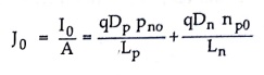
The
diffusion length for the holes and electrons is given by,
Lp = √(Dpτp)
Ln = √(Dnτn)
np0 = ni2
/ NA
Pno = ni2
/ ND
….. by law of mass action
Lp = √(Dpτp)
= √[10×10‒4×5×10‒7] = 2.236×10‒5
Ln = √(Dnτn)
= √[25×10‒4×5×10‒7] = 3.535×10‒5
np0 = ni2
/ NA = (1.5×10¹⁶)2 /
1022 =2.25×10¹⁰
Pno = ni2
/ ND= (1.5×10¹⁶)2 / 1022
=2.25×10¹⁰
q
= 16×10‒19 C and using in (1),
J0
= 1.6×10‒19 [ (10×10‒4×2.25×1010 / 2.236×10‒5
) + (25×10-4×2.25×1010 /3.535×10‒5) ]
= 4.15×10‒7A/m2
i.e.4.15×10‒11
A/cm2
Comment:
Ideally reverse saturation current density is very small. If the area of cross‒section
A is given as 2×10‒8 m2 then I0 becomes J0
× A i.e., 4.15×10‒7×2×10‒8 = 8.3119×10‒15 A.
Thus ideally reverse saturation current is also very small.
Review
Question
1. Derive the p‒n diode current equation.
Electron Devices: Chapter 2: PN Junction Diodes : Tag: electronics : - Derivation of V‒I Characteristics of PN Junction Diode (Diode Current Equation)
Electron Devices: Chapter 2: PN Junction Diodes
Under Subject

Electron Devices
EC25C01 2nd Semester ECE Dept | 2025 Regulation | 2nd Semester 2025 Regulation
Related Subjects

English Essentials II
EN25C02 2nd Semester | 2025 Regulation | 2nd Semester 2025 Regulation

Tamils and Technology தமிழர்களும் தொழில்நுட்பமும்
UC25H02 2nd Semester | 2025 Regulation | 2nd Semester 2025 Regulation

Linear Algebra
MA25C02 2nd Semester | 2025 Regulation
Electron Devices
EC25C01 2nd Semester ECE Dept | 2025 Regulation | 2nd Semester 2025 Regulation

Data Structures using CPlusPlus
CS25C05 2nd Semester ECE Dept | 2025 Regulation | 2nd Semester 2025 Regulation

Circuits and Network Analysis
EC25C02 2nd Semester ECE Dept | 2025 Regulation | 2nd Semester 2025 Regulation

Re-Engineering for Innovation
ME25C05 2nd Semester | 2025 Regulation | 2nd Semester 2025 Regulation

Engineering Drawing - Laboratory
ME25C01 2nd Semester | 2025 Regulation | 2nd Semester 2025 Regulation

Data Structures using CPlusPlus - Laboratory
CS25C05 2nd Semester ECE Dept | 2025 Regulation | 2nd Semester 2025 Regulation

Devices and Circuits Laboratory
EC25C03 2nd Semester ECE Dept | 2025 Regulation | 2nd Semester 2025 Regulation