Electron Devices: Chapter 2: PN Junction Diodes
Theory of PN Junction
Questions: 1. Explain the theory of p‒n junction. 2. Explain the formation of depletion region in an unbiased p‒n junction, with the help of neat sketch. 3. Briefly explain about depletion region and barrier voltage of a PN junction.
Theory
of P‒N Junction
•
In a p‒n junction, on p‒side there are large number of holes while on n‒side
there are large number of electrons. Hence the overall there is nonuniform
distribution of charge carriers.
•
When such nonuniform distribution exists then the charge carriers moving from
high concentration area towards the low concentration area. This is called
diffusion.
•
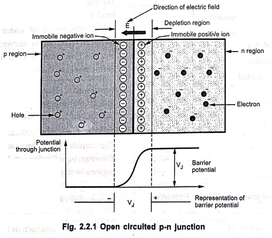
In unbiased p‒n junction, the majority holes on p side start diffusing into n
side while the majority free electrons on n side start diffusing into p side.
•
In n region, the holes difusing from n‒side, recombine with free electrons. Thus
due to additional positively charged holes, these atoms on n‒side become
positive immobile ions, just near the junction in n region.
•
In p region, the free electrons diffusing from n‒side, recombine with the holes
of the atoms. Thus due to gain of additional negatively charged free electrons,
these atoms become negative immobile ions, just near the junction in p‒region.
•
As more holes diffuse on n side, large immobile positive charge accumulates
near the junction on n side. This positive charge repels the positively charged
holes and the diffusion of holes stops.
•
Similarly large negative charge accumulates near the junction on p side. This
negative charge repels the negatively charged electrons and the diffusion of
electrons stops.
• Thus there exists a wall near the junction with negative immobile charge on p side and positive immobile charge on n side. There are no charge carriers in this region. The region is depleted off the charge carriers hence called depletion region, depletion layer or space charge region. The depletion region is shown in Fig. 2.2.1.
•
In equilibrium condition, the depletion region gets widened upto a point where
no further electrons or holes can cross the junction. Thus it acts as a
barrier.
Barrier Potential
•
Due to immobile positive ions on n side and immobile negative ions on p side,
there exists an electric field across the junction.
•
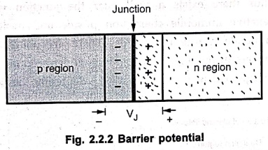
This creates potential difference across the depletion region which acts as a
barrier. This is called barrier potential, junction potential, built‒in
potential or cut‒in potential of p‒n junction.
•
It is denoted as VJ and is shown in Fig. 2.2.2. It is also called
height of the depletion region and also denoted as VO or Vγ.
•
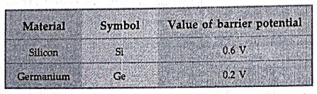
The barrier potential depends on,
1.
Type of semiconductor
2.
Donor impurity added
3.
Acceptor impurity added
4.
Temperature
Effect of Temperature on Barrier Potential
The
physical distance from one side to other side of the depletion region is called
width of the depletion region. Practically width of the depletion region is
about 0.5 to 1 micron. (1 micron = 10‒6 m).
•
As temperature increases, the width of the depletion region decreases.
•
Thus as temperature increases, the barrier potential decreases.
•
The barrier potential decreases by approximately 2.5 mV per degree celcius rise
in temperature.
Review
Questions
1. Explain the theory of p‒n junction.
2. Explain the formation of depletion region in an unbiased p‒n
junction, with the help of neat sketch.
3. Briefly explain about depletion region and barrier voltage of
a PN junction.
Electron Devices: Chapter 2: PN Junction Diodes : Tag: electronics : - Theory of PN Junction
Electron Devices: Chapter 2: PN Junction Diodes
Under Subject

Electron Devices
EC25C01 2nd Semester ECE Dept | 2025 Regulation | 2nd Semester 2025 Regulation
Related Subjects

English Essentials II
EN25C02 2nd Semester | 2025 Regulation | 2nd Semester 2025 Regulation

Tamils and Technology தமிழர்களும் தொழில்நுட்பமும்
UC25H02 2nd Semester | 2025 Regulation | 2nd Semester 2025 Regulation

Linear Algebra
MA25C02 2nd Semester | 2025 Regulation
Electron Devices
EC25C01 2nd Semester ECE Dept | 2025 Regulation | 2nd Semester 2025 Regulation

Data Structures using CPlusPlus
CS25C05 2nd Semester ECE Dept | 2025 Regulation | 2nd Semester 2025 Regulation

Circuits and Network Analysis
EC25C02 2nd Semester ECE Dept | 2025 Regulation | 2nd Semester 2025 Regulation

Re-Engineering for Innovation
ME25C05 2nd Semester | 2025 Regulation | 2nd Semester 2025 Regulation

Engineering Drawing - Laboratory
ME25C01 2nd Semester | 2025 Regulation | 2nd Semester 2025 Regulation

Data Structures using CPlusPlus - Laboratory
CS25C05 2nd Semester ECE Dept | 2025 Regulation | 2nd Semester 2025 Regulation

Devices and Circuits Laboratory
EC25C03 2nd Semester ECE Dept | 2025 Regulation | 2nd Semester 2025 Regulation