Electron Devices: Chapter 2: PN Junction Diodes
Reverse Biasing of PN Junction Diode

Questions: 1. With a neat diagram explain the working of a PN junction diode in reverse bias condition. 2. Explain the V‒I charactersics of diode in reverse biased mode. 3. Explain briefly : i) Avalanche breakdown ii) Zener breakdown. 4. With necessary diagram, describe the characteristics of a reverse biased PN junction diode. Index: 1. Operation of Reverse Biased Diode 2. Breakdown Mechanisms 3. Reverse Characteristics of P‒N Junction Diode 4. Reverse Resistance of Diode
Reverse
Biasing of P‒N Junction Diode
•
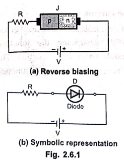
If an external d.c. voltage is connected in such a way that the p‒region
terminal of a p‒n junction is connected to the negative of the battery and the
n‒region terminal of a p‒n junction is connected to the positive terminal of
the battery, the biasing condition is called reverse biasing of a p‒n junction.
Key
Point: Reverse biasing means connecting p‒region to ‒ve
and n‒region to +ve of the battery.
•
Fig. 2.6.1 (a) shows the connection of a reverse biasing of a p‒n junction
while Fig. 2.6.1 (b) shows the symbolic representation of a reverse biased
diode.
1. Operation of Reverse Biased Diode
•
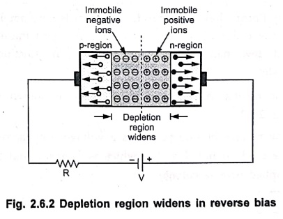
When the p‒n junction is reverse biased the negative terminal attracts the
holes in the p‒region, away from the junction.
•
The positive terminal attracts the free electrons in the n‒region away from the
junction.
•
No charge carrier is able to cross the junction.
•
As electrons and holes both move away from the junction, the depletion region
widens.
•
This creates more positive ions and hence more positive charge in the n‒region
and more negative ions and hence more negative charge in the n‒region. This is
because the applied voltage helps the barrier potential. This is shown in Fig.
2.6.2.
Key
Point: Reverse biasing increases the width of the
depletion region.
•
As depletion region widens, barrier potential across the junction also
increases. However, this process cannot continue for long time. In the steady
state, majority current ceases as holes and electrons stop moving away from the
junction.
•
The polarities of barrier potential are same as that of the applied voltage.
•
Due to increased barrier potential, the positive side drags the electrons from
p‒region towards the positive of battery. Similarly negative side of barrier
potential drags the holes from n‒region towards the negative of battery.
•
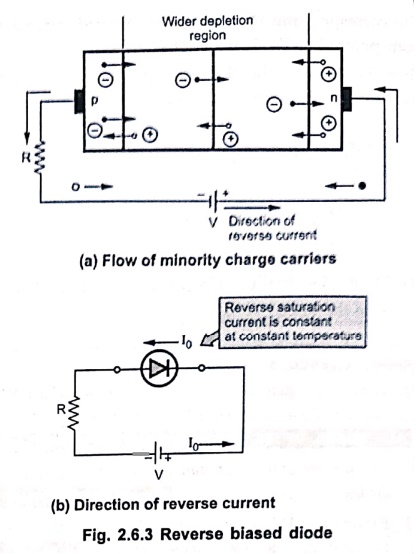
The electrons on p side and holes on n side are minority charge carriers, which
constitute the current in reverse biased condition. Thus reverse conduction
takes place.
•
The reverse current flows due to minority charge carriers which are small in
number. Hence reverse current is always very small.
Key
Point: The generation of minority charge carriers depends
on the temperature and not on the applied reverse bias voltage. Thus the
reverse current depends on the temperature i.e. thermal generation and not on
the reverse voltage applied.
•
For a constant temperature, the reverse current is almost constant though
reverse voltage is increased upto a certain limit. Hence it is called reverse
saturation current and denoted as I0.
Key
Point: Reverse saturation current is very small of the
order of few microamperes for germanium and few nanoamperes for silicon p‒n
junction diodes.
•
The reverse current and its direction is shown in Fig. 2.6.3.
•
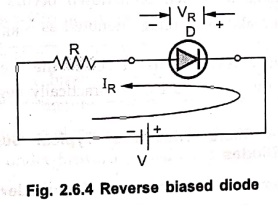
The reverse biasing produces a voltage drop across the diode denoted as VR
which is almost equal to applied reverse voltage.
2. Breakdown Mechanisms
•
If reverse voltage is increased beyond particular value, large reverse current
can flow damaging the diode. This is called reverse breakdown of a diode.
•
Such a reverse breakdown of a diode can take place due to the following two
effects,
1.
Avalanche effect and
2.
Zener effect
Breakdown due to the Avalanche Effect:
•
If reverse voltage is increased, at a particular value, velocity of minority
carriers increases.
•
Due to the kinetic energy associated with the minority carriers, more minority
carriers are generated when there is collision of minority carriers with the
atoms. The collision make the electrons to break the co‒valent bonds.
•
These electrons are available as minority carriers and get accelerated due to
high reverse voltage. They again collide with another atoms to generate more
minority carriers. This is called carrier multiplication.
•
Finally large number of minority carriers move across the junction, breaking
the p‒n junction. These large number of minority carriers give rise to a very
high reverse current.
•
This effect is called avalanche effect and the mechanism of destroying the
junction is called reverse breakdown of a p‒n junction. The voltage at which
the breakdown of a p‒n junction occurs is called reverse breakdown voltage.
Breakdown due to the Zener Effect:
•
Electric field is voltage per distance and due to narrow depletion region and
high reverse voltage, it is intense.
•
Such an intense field is enough to pull the electrons out of the valence bands
of the stable atoms.
•
Such a creation of free electrons is called zener effect which is different
than the avalanche effect. These minority carriers constitute very large
current and mechanism is called zener breakdown.
•
These effects are required to be considered for special diodes such as Zener
diode as such diodes are always always operated in reverse breakdown condition.
3. Reverse Characteristics of P‒N Junction Diode
•
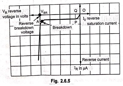
Fig. 2.6.4 shows the reverse biased diode. The reverse voltage across the diode
is VR while the current flowing is reverse current IR
flowing due to minority charge carriers.
• The graph of IR against VR is called reverse characteristics of a diode.
•
The polarity of reverse voltage applied is opposite to that of forward voltage.
Hence in practice reverse voltage is taken as negative.
•
Similarly the reverse saturation current is due to minority carriers and is
opposite to the forward current. Hence in practice reverse saturation current
is also taken as negative.
•
Hence the reverse characteristics is plotted in the third quadrant as shown in
Fig. 2.6.5.
Key
Point: Typically the reverse breakdown voltage is greater
than 50 V for normal p‒n junctions.
•
As reverse voltage is increased, reverse current increases initially but after
a certain voltage, the current remains constant equal to reverse saturation
current I0 though reverse voltage is increased.
•
The point A where breakdown occurs and reverse current increases rapidly is
called knee of the reverse characteristics.
•
The voltage corresponding to point A is called reverse breakdown voltage VBR
of diode.
4. Reverse Resistance of Diode
•
The p‒n junction offers large resistance in the reverse biased condition called
reverse resistance. This is also defined in two ways.
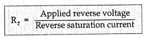
1. Reverse static
resistance: This is reverse resistance under d.c.
conditions, denoted as Rr It is the ratio of applied reverse voltage
to the reverse saturation current I0.
Rr = Applied reverse
voltage / Reverse saturation current
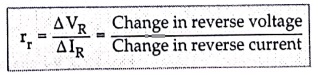
2. Reverse dynamic
resistance: This is the reverse resistance under
the a.c. conditions, denoted as rr. It is the ratio of incremental
change in the reverse voltage applied to the corresponding change in the
reverse current.
rr = ΔVR / ΔIR
= Change in reverse voltage / Change in reverse current
•
The dynamic resistance is most important in practice whether the junction is
forward or reverse biased.
Review Questions
1. With a neat diagram explain the working of a PN junction
diode in reverse bias condition.
2. Explain the V‒I charactersics of diode in reverse biased
mode.
3. Explain briefly : i) Avalanche breakdown ii) Zener breakdown.
4. With necessary diagram, describe the characteristics of a
reverse biased PN junction diode.
Electron Devices: Chapter 2: PN Junction Diodes : Tag: electronics : - Reverse Biasing of PN Junction Diode
Electron Devices: Chapter 2: PN Junction Diodes
Under Subject

Electron Devices
EC25C01 2nd Semester ECE Dept | 2025 Regulation | 2nd Semester 2025 Regulation
Related Subjects

English Essentials II
EN25C02 2nd Semester | 2025 Regulation | 2nd Semester 2025 Regulation

Tamils and Technology தமிழர்களும் தொழில்நுட்பமும்
UC25H02 2nd Semester | 2025 Regulation | 2nd Semester 2025 Regulation

Linear Algebra
MA25C02 2nd Semester | 2025 Regulation
Electron Devices
EC25C01 2nd Semester ECE Dept | 2025 Regulation | 2nd Semester 2025 Regulation

Data Structures using CPlusPlus
CS25C05 2nd Semester ECE Dept | 2025 Regulation | 2nd Semester 2025 Regulation

Circuits and Network Analysis
EC25C02 2nd Semester ECE Dept | 2025 Regulation | 2nd Semester 2025 Regulation

Re-Engineering for Innovation
ME25C05 2nd Semester | 2025 Regulation | 2nd Semester 2025 Regulation

Engineering Drawing - Laboratory
ME25C01 2nd Semester | 2025 Regulation | 2nd Semester 2025 Regulation

Data Structures using CPlusPlus - Laboratory
CS25C05 2nd Semester ECE Dept | 2025 Regulation | 2nd Semester 2025 Regulation

Devices and Circuits Laboratory
EC25C03 2nd Semester ECE Dept | 2025 Regulation | 2nd Semester 2025 Regulation