Electron Devices: Chapter 2: PN Junction Diodes
The PN Junction Diode
Symbol, Construction, Working principle
Questions: 1. Draw the symbol of p‒n junction diode. What are ohmic contacts ? 2. What is biasing of p‒n junction diode ? 3. Discuss the construction of p‒n junction diode.
The
P‒N Junction Diode
•
The p‒n junction forms a popular semiconductor device called p‒n junction
diode.
•
The p‒n junction has two terminals called electrodes, one each from p‒region
and n‒region. Due to the two electrodes it is called diode i.e. di + electrode.
•
To connect the n and p‒regions to the external terminals, a metal is applied to
the heavily doped n and p‒type semiconductor regions. Such a contact between a
metal and a heavily semiconductor is called ohmic contact.
•
Such an ohmic contact has two important properties,
1.
It conducts current equally in both the directions.
2.
The drop across the contact is very small, which do not affect the performance
of the device.
•
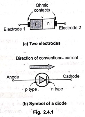
Fig. 2.4.1 (a) shows schematic arrangement of p‒n junction diode while Fig.
2.4.1 (b) shows the symbol of p‒n junction diode.
•
The p‒region acts as anode while the n‒region acts as cathode. The arrowhead in
the symbol indicates the direction of the conventional current, which can flow
when an external voltage is connected in a specific manner across the diode.
•
Applying external d.c. voltage to any electronic device is called biasing.
•
The usefulness of p‒n junction lies in the fact that it allows current flow
only in one direction, under biased condition.
•
Depending upon the polarity of the d.c. voltage externally applied to it, the
biasing is classified as Forward biasing and Reverse biasing.
Review
Questions
1. Draw the symbol of p‒n junction diode. What are ohmic
contacts ?
2. What is biasing of p‒n junction diode ?
3. Discuss the construction of p‒n junction diode.
Electron Devices: Chapter 2: PN Junction Diodes : Tag: electronics : Symbol, Construction, Working principle - The PN Junction Diode
Electron Devices: Chapter 2: PN Junction Diodes
Under Subject

Electron Devices
EC25C01 2nd Semester ECE Dept | 2025 Regulation | 2nd Semester 2025 Regulation
Related Subjects

English Essentials II
EN25C02 2nd Semester | 2025 Regulation | 2nd Semester 2025 Regulation

Tamils and Technology தமிழர்களும் தொழில்நுட்பமும்
UC25H02 2nd Semester | 2025 Regulation | 2nd Semester 2025 Regulation

Linear Algebra
MA25C02 2nd Semester | 2025 Regulation
Electron Devices
EC25C01 2nd Semester ECE Dept | 2025 Regulation | 2nd Semester 2025 Regulation

Data Structures using CPlusPlus
CS25C05 2nd Semester ECE Dept | 2025 Regulation | 2nd Semester 2025 Regulation

Circuits and Network Analysis
EC25C02 2nd Semester ECE Dept | 2025 Regulation | 2nd Semester 2025 Regulation

Re-Engineering for Innovation
ME25C05 2nd Semester | 2025 Regulation | 2nd Semester 2025 Regulation

Engineering Drawing - Laboratory
ME25C01 2nd Semester | 2025 Regulation | 2nd Semester 2025 Regulation

Data Structures using CPlusPlus - Laboratory
CS25C05 2nd Semester ECE Dept | 2025 Regulation | 2nd Semester 2025 Regulation

Devices and Circuits Laboratory
EC25C03 2nd Semester ECE Dept | 2025 Regulation | 2nd Semester 2025 Regulation