Electron Devices: Chapter 2: PN Junction Diodes
Transition Capacitance of PN Junction Diodes
Questions: 1. Explain the concept of transition capacitance of p‒n junction diode. 2. Derive the expression for the capacitance of p‒n junction diode.
Transition
Capacitance (CT)
•
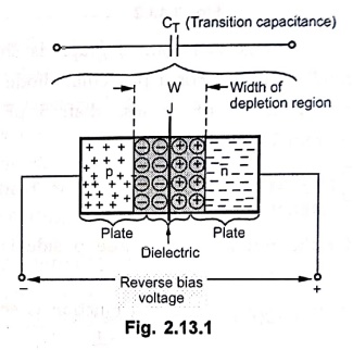
When a diode is reverse biased, the width of the depletion region increases. So
there are more positive and negative charges present in the depletion region.
•
Due to this, the p‒region and n‒region act like the plates of capacitor while
the depletion region acts like dielectric.
•
Thus there exists a capacitance at the p‒n junction called transition
capacitance, junction capacitance, space charge capacitance, barrier
capacitance or depletion region capacitance. It is denoted as CT.
•
Mathematically it is given by the expression,
Ст = εΑ /
W
……... (2.13.1)
where
ε
= Permittivity of semiconductor
=
ε0εr
ε0
= 1 / 36π×109 = 8.849×10‒12 F/m
εr
= Relative permittivity of semiconductor = 16 for Ge, 12 for Si
A
= Area of cross section
W
= Width of depletion region
•
As the reverse biased applied to the diode increases, the width of the
depletion region (W) increases. Thus the transition capacitance CT
decreases.
•
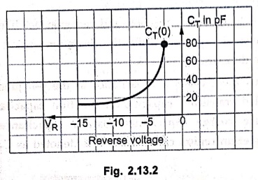
In short, the capacitance can be controlled by the applied voltage. The
variation of CT with respect to the applied reverse bias voltage is
shown in Fig. 2.13.2.
•
As reverse voltage is negative, graph is shown in the second quadrant. For a
particular diode shown, CT varies from 80 pF to less than 5 pF as VR
changes from 2 V to 15 V.
1. Derivation of Expression for Transition Capacitance
•
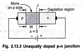
Consider the p‒n junction whose p side is lightly doped than n side.
•
Such an unequally doped p‒n junction is shown in Fig. 2.13.3, which is reverse
biased.
•
The depletion region penetrates more on lightly doped side hence its width is
more on p side.
•
Practically it can be assumed that concentration of impurity on both sides is
such that the entire depletion region is on p side only.
•
Let NA = Concentration of acceptor impurity on p side.
•
The relation between potential V and charge density NA is given by
Poisson's equation as,
d2V / dx2 = qNA
/ ε
….. x=Distance measured from junction
ε = ε0 εr
= Permittivity of semiconductor
where
ε0 = 8.854 × 10‒12 F/m
εr = 16 for Ge and 12 for Si
•
Integrating above equation with respect x,
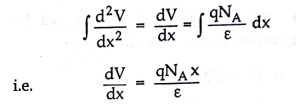 ...(2.13.2)
•
But dV/dx is the electric field E over the region x = 0 to x = W over which
depletion region exists.
E
= qNAx / ε
……. q = Charge on each electron
...(2.13.3)
•
Integrating equation (2.13.2)
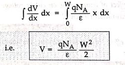 ...(2.13.4)
•
At x=W, V = VB = Barrier potential which is the difference between
junction potential VJ and applied reverse bias V i.e. VB
= VJ− V
...(2.13.5)
•
V must be taken as negative as reverse biased. Hence as V becomes more
negative, VB = VJ − (− V) = VJ + V increases.
•
Using in equation (2.13.4),
VB
= qNA/ε . W2/2
W ∝ √VB
...(2.13.6)
The
width of depletion region increases as applied reverse bias voltage increases
•
If A is the area of cross‒section of junction, W is the width then net charge Q
in the distance W is,
Q = NA × Volume × q = NA
A W q ...(2.13.7)
•
Differentiating equation (2.13.4) with respect to V,
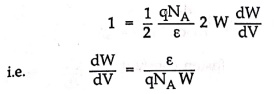
...(2.13.8)
•
Differentiating equation (2.13.7) with respect to V,
dQ
/ dV = NA A (dW/dV) q
...(2.13.9)
•
Using equation (2.13.8) in (2.13.9) and dQ/dV = CT
Ст = εA/W
= Transition capacitance
………….. (2.13.10)
•
Thus CT = 1/W and hence as reverse bias increases, the width of the
depletion region W increases and hence transition capacitance CT
decreases.
Ex. 2.13.1: A germanium diode has a contact
potential of 0.2 V and concentration of acceptor impurity is 3×10²⁰/m3.
Area of cross‒section of junction is 1 mm2 and εr = 16.
Calculate width of depletion region and transition capacitance for reverse bias
of a) 0.1 V and b) 10 V (Assume charge on each electron as 1.6 × 10‒19C)
Solution:
V1 = 0.2 V, NA = 3 × 10²⁰/m3,
A = 1 mm2, εr = 16
a)
V = ‒0.1 V
……… Negative as reverse bias
VB = VJ‒ V = 0.2 − (−
0.1) = 0.3 V
VB = qNA/ε . W2/2
i.e.
0.3 = (1.6 × 10‒19 × 3 × 1020)
/ (8.854 × 10‒12 × 16) . W2/2
W = 1.33 μm,
Ст = εA/W = (ε×1×10‒19)
/ (1.33×10‒6) = 106.45 pF
b)
V = ‒10V
hence
VB
= VJ ‒ V = 0.2 ‒ (‒10) = 10.2 V
10.2 = [ 1.6 × 10‒19 × 3 × 1020
] / [8.854 × 10‒12 × 16] × [W2/2]
i.e.
W
= 7.75 μm
Ст
= εA
=
( 8854 × 10‒12 × 16 × 1 × 10‒6 ) / (7.75 × 10‒6)
=
18.25 pF
Thus
as reverse bias voltage increases, width of depletion region increases while
transition capacitance decreases.
Review
Questions
1. Explain the concept of transition capacitance of p‒n junction
diode.
2. Derive the expression for the capacitance of p‒n junction
diode.
Electron Devices: Chapter 2: PN Junction Diodes : Tag: electronics : - Transition Capacitance of PN Junction Diodes
Electron Devices: Chapter 2: PN Junction Diodes
Under Subject

Electron Devices
EC25C01 2nd Semester ECE Dept | 2025 Regulation | 2nd Semester 2025 Regulation
Related Subjects

English Essentials II
EN25C02 2nd Semester | 2025 Regulation | 2nd Semester 2025 Regulation

Tamils and Technology தமிழர்களும் தொழில்நுட்பமும்
UC25H02 2nd Semester | 2025 Regulation | 2nd Semester 2025 Regulation

Linear Algebra
MA25C02 2nd Semester | 2025 Regulation
Electron Devices
EC25C01 2nd Semester ECE Dept | 2025 Regulation | 2nd Semester 2025 Regulation

Data Structures using CPlusPlus
CS25C05 2nd Semester ECE Dept | 2025 Regulation | 2nd Semester 2025 Regulation

Circuits and Network Analysis
EC25C02 2nd Semester ECE Dept | 2025 Regulation | 2nd Semester 2025 Regulation

Re-Engineering for Innovation
ME25C05 2nd Semester | 2025 Regulation | 2nd Semester 2025 Regulation

Engineering Drawing - Laboratory
ME25C01 2nd Semester | 2025 Regulation | 2nd Semester 2025 Regulation

Data Structures using CPlusPlus - Laboratory
CS25C05 2nd Semester ECE Dept | 2025 Regulation | 2nd Semester 2025 Regulation

Devices and Circuits Laboratory
EC25C03 2nd Semester ECE Dept | 2025 Regulation | 2nd Semester 2025 Regulation