Electron Devices: Chapter 2: PN Junction Diodes
pn Diode Currents
Explain the current components in a p‒n junction diode.
p‒n
Diode Currents
•
It is indicated earlier that when a p‒n junction diode is forward biased a
large forward current flows, which is mainly due to majority carriers. The
depletion region near the junction is very very small, under forward biased
condition.
•
In forward biased condition holes get diffused into n‒side from p‒side while
electrons get diffused into p‒side from n side.
•
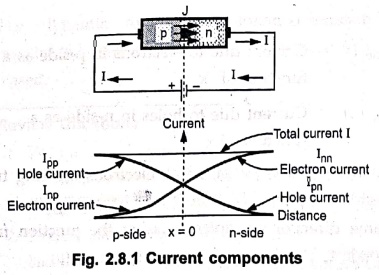
So on p‒side, the current carried by electrons which is diffusion current due
to minority carriers, decreases exponentially with respect to distance measured
from the junction. This current due to electrons, on p‒side which are minority
carriers is denoted as Inp.
•
Similarly holes from p‒side diffuse into n‒side carry current which decreases
exponentially with respect to distance measured from the junction. This current
due to holes on n‒side, which are minority carriers is denoted as Ipn.
•
If distance is denoted by x then,
Inp
(x) = Current due to electrons in p‒side as a function of x
Ipn
(x) = Current due to holes in n‒side as a function of x
•
At the junction i.e. at x = 0, electrons crossing from n‒side to p‒side
constitute a current, Iap (0) in the same direction as holes
crossing the junction from p‒side to n‒side constitute a current, Ipn(0).
•
Hence the current at the junction is the total conventional current I flowing
through the circuit.
I = Ipn(0) + Inp (0) .. (2.8.1)
•
Now Ipn (x) decreases on n‒side as we move away from junction on n‒side.
Similarly Inp (x) decreases on p‒side as we move away from junction
on p‒side.
•
But as the entire circuit is a series circuit, the total current must be
maintained at I, independent of x.
•
This indicates that on p‒side there exists one more current component which is
due to holes on p‒side which are the majority carriers. It is denoted by Ipp(x)
and the addition of the two currents on p‒side is total current I.
Ipp (x) = Current due to holes in p‒side.
•
Similarly on n‒side, there exists one more current component which is due to
electrons on n‒side, which are the majority carriers. It is denoted as Inn(x)
and the addition of the two currents on n‒side is total current I.
Inn(x) = Current due to electrons
in n‒side.
On p‒side, I = Ipp(x) + Inp(x) …………(2.8.2)
On
n‒side, I = Inn(x) + Ipn(x) ……… (2.8.3)
•
These current components are plotted as a function of distance in Fig. 2.8.1.
•
The current Ipp decreases towards the junction, at the junction
enters the n side and becomes Ipn which further decreases
exponentially.
•
Similarly the current Inn decreases towards the junction, at the
junction enters the p‒side and becomes Inp which also further
decreases exponentially.
Key
Point: In forward bias condition, the current enters the p‒side
as a hole current and leaves the n‒side as an electron current, of the same
magnitude.
•
So sum of the currents carried by electrons and holes at any point inside the
diode is always constant equal to total forward current I. But the proportion
due to holes and electrons in constituting the current varies with the
distance, from the junction.
Review Question
1. Explain the current components in a p‒n junction diode.
Electron Devices: Chapter 2: PN Junction Diodes : Tag: electronics : - pn Diode Currents
Electron Devices: Chapter 2: PN Junction Diodes
Under Subject

Electron Devices
EC25C01 2nd Semester ECE Dept | 2025 Regulation | 2nd Semester 2025 Regulation
Related Subjects

English Essentials II
EN25C02 2nd Semester | 2025 Regulation | 2nd Semester 2025 Regulation

Tamils and Technology தமிழர்களும் தொழில்நுட்பமும்
UC25H02 2nd Semester | 2025 Regulation | 2nd Semester 2025 Regulation

Linear Algebra
MA25C02 2nd Semester | 2025 Regulation
Electron Devices
EC25C01 2nd Semester ECE Dept | 2025 Regulation | 2nd Semester 2025 Regulation

Data Structures using CPlusPlus
CS25C05 2nd Semester ECE Dept | 2025 Regulation | 2nd Semester 2025 Regulation

Circuits and Network Analysis
EC25C02 2nd Semester ECE Dept | 2025 Regulation | 2nd Semester 2025 Regulation

Re-Engineering for Innovation
ME25C05 2nd Semester | 2025 Regulation | 2nd Semester 2025 Regulation

Engineering Drawing - Laboratory
ME25C01 2nd Semester | 2025 Regulation | 2nd Semester 2025 Regulation

Data Structures using CPlusPlus - Laboratory
CS25C05 2nd Semester ECE Dept | 2025 Regulation | 2nd Semester 2025 Regulation

Devices and Circuits Laboratory
EC25C03 2nd Semester ECE Dept | 2025 Regulation | 2nd Semester 2025 Regulation