Electron Devices: Chapter 2: PN Junction Diodes
Energy Band Structure of Open Circuited PN Junction
Questions: 1. Draw and explain the energy band structure for open circuited p‒n junction. 2. Derive the expression for the built in potential barrier. 3. Important Example Solved Problems
Energy
Band Structure of Open Circuited P‒N Junction
•
The Fermi level in n type materal lies just below the conduction band while in
p‒type material, it lies just above the valence band.
•
When p‒n junction is formed, the diffuson starts. The charges get adjusted so
as to equalise the Fermi level in the two parts of p‒n junction. This is
similar to the adjustment of water levels in two tanks of unequal level, when
connected to each other. The charges flow from p to n and n to p side till, the
Fermi level on the two sides get lined up.
Key
Point: The transfer of charges does not disturb the
relative positions of conduction band, valence band and Fermi level in any
region either p or n.
•
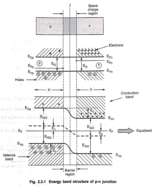
The transfer of charges and energy band structure showing equalisation of Fermi
levels in p and n regions is shown in Fig. 2.3.1.
•
In p region, the Fermi level EFp is near Evp just above
edge of valence band.
• In n region, the Fermi level EFn is near ECn just below edge of conduction band.
•
And there is difference between levels of EFn and EFP.
•
The transport of charges, the edge of conduction band Ecp in the p
type material becomes higher than ECn in the n type material.
Similarly the edge of valence band Evp in p type is higher than EVn
in n type material. Thus there is a shift of E1 in the Fermi level
on p side while there is a shift of E2 in the Fermi level on n side
from their intrinsic levels. (i.e. centre of EC and EV).
•
This adjusts the Fermi level on n and p side to get equivalent Fermi level EF
for the p‒n junction.
•
The total shift in energy E0 is E1 + E2 which
is responsible to produce contact difference of potential across the junction.
This is nothing but barrier potential or junction potential or contact
potential given by,
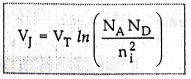
VJ = VT In (NAND
/ ni2)
where
VT= kT
Where
NA
= Concentration of acceptor impurity
ND
= Concentration of donor impurity
ni
= Intrinsic concentration
k
= Boltzmann's constant = 8.62 × 10⁵ eV/°K
1. Width of Space Charge Region
•
As the reverse bias voltage VR increases, the width of the space
charge region increase.
•
Many times it is necessary to calculate the width of the space charge region
denoted as W.
•
While calculating W, it is necessary to consider total potential barrier
instead of the built in potential VJ.
•
The total potential barrier is the difference between the junction potential
and applied reverse bias.
VB = VJ ‒ (VR)
•
But VR is taken as negative as reverse bias hence we can write,
VB = VJ + VR
=
Total potential barrier
………..(2.3.1)
where
VR = Magnitude at the reverse bias
voltage.
•
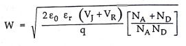
The width of the space charge region is given by
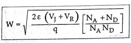
…………. (2.3.2)
Where
q
= Charge on each electron
=
1.6×10‒19 C
ε
= ε0 εr,
εr = 11.7 for Si,
εr
= 16 for Ge
Ex. 2.3.1 Consider a Si PN junction at T = 300° K with doping concentrations of NA =1016 cm‒3 and ND = 1015 cm-3. Assume that ni = 1.5×1010 cm-3. Calculate width of the space charge region in a PN junction, when a reverse bias voltage VR = 5 V is applied.
Solution:
T
= 300°K,
NA
=1016 /cm3, ND = 1015 / cm3,
ni =1.5×10¹⁰ /cm3,
VR = 5V, εr = 11.7 for Si,
q = 1.6×10‒19
VJ
= VT In [NAND / ni2]
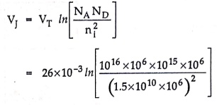
=
26×10‒3 In [ (1016×106×1015×106)
/ (1.5×1010×106)2 ]
=
0.637 V
VB
= VJ+VR = 5 + 0.637 = 5.637 V
=
2.833 μm
Note
that NA =1016/cm3 = 1016 × 106/m3
=1022/m3
2. Derivation of Potential Barrier
•
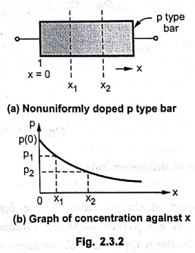
Consider non uniformly doped p type bar as shown in Fig. 2.3.2 (a).
•
Fig 2.3.2 (b) shows the graph of concentration of holes against distance x.
•
There exists potential difference between any two points of such a bar.
•
Let concentration at x = x1 is P1 and concentration at
x=x2 is P2.
•
Let potential at x1 = V1 and at x2 = V2.
•
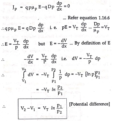
The net current through the bar is zero hence
•
In p‒n junction, there is abrupt change in the concentration of holes from Pp
to Pn.
P1 ≈ PP ≈ NA
and P2 =Pn
while
V2
‒V1 = VJ
•
Using in equation (2.3.3),
VJ = VT In (NA/Pn)
= Potential barrier
•
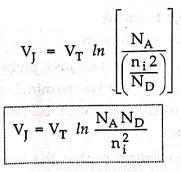
According to law of mass action, nn ×Pn = ni2
Pn = ni2/nn
but nn = ND hence Pn = ni2/ND
•
This is the required expression for the built in potential barrier.
Ex. 2.3.2 Calculate the built in potential
barrier in a PN junction. Consider a silicon PN junction at 300 °K with doping
densities NA =1×1018 cm-3 and ND
=1×1015 cm-3. Assume ni =1.5×10¹⁰
cm-3.
Solution:
T
= 300 °K, NA =1×10¹⁸ / cm3 = 1×1024
/m3,
ND
=1×10¹⁵ / cm3 =1×10²¹/m3, ni
ni =1×10¹⁵ / cm3 = 1×10²¹/m3
VT
= 0.0259 V at T = 300 °K
VJ
= VT In[NAND /ni2]
=
0.178 V
Review
Questions
1. Draw and explain the energy band structure for open circuited
p‒n junction.
2. Derive the expression for the built in potential barrier.
3. Consider a step graded germanium p‒n junction. It has ND=103
NA and NA corresponds to 1 atom per 108
germanium atoms. Calculate the junction potential.
Assume ni = 2.5×103 cm3, atom
density of Ge = 4.4 × 10²² atoms per cm3. [Ans. : 0.328 V]
Electron Devices: Chapter 2: PN Junction Diodes : Tag: electronics : - Energy Band Structure of Open Circuited PN Junction
Electron Devices: Chapter 2: PN Junction Diodes
Under Subject

Electron Devices
EC25C01 2nd Semester ECE Dept | 2025 Regulation | 2nd Semester 2025 Regulation
Related Subjects

English Essentials II
EN25C02 2nd Semester | 2025 Regulation | 2nd Semester 2025 Regulation

Tamils and Technology தமிழர்களும் தொழில்நுட்பமும்
UC25H02 2nd Semester | 2025 Regulation | 2nd Semester 2025 Regulation

Linear Algebra
MA25C02 2nd Semester | 2025 Regulation
Electron Devices
EC25C01 2nd Semester ECE Dept | 2025 Regulation | 2nd Semester 2025 Regulation

Data Structures using CPlusPlus
CS25C05 2nd Semester ECE Dept | 2025 Regulation | 2nd Semester 2025 Regulation

Circuits and Network Analysis
EC25C02 2nd Semester ECE Dept | 2025 Regulation | 2nd Semester 2025 Regulation

Re-Engineering for Innovation
ME25C05 2nd Semester | 2025 Regulation | 2nd Semester 2025 Regulation

Engineering Drawing - Laboratory
ME25C01 2nd Semester | 2025 Regulation | 2nd Semester 2025 Regulation

Data Structures using CPlusPlus - Laboratory
CS25C05 2nd Semester ECE Dept | 2025 Regulation | 2nd Semester 2025 Regulation

Devices and Circuits Laboratory
EC25C03 2nd Semester ECE Dept | 2025 Regulation | 2nd Semester 2025 Regulation