Electron Devices: Chapter 2: PN Junction Diodes
Basic Structure of PN Junction
Questions: 1. What is a p‒n junction? 2. Explain the basic structure of p‒n junction.
Basic Structure of P‒N Junction
•
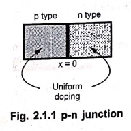
Fig. 2.1.1 shows the p‒n junction at x = 0, with uniform doping in each region.
•
Both types of charge carriers, majority as well as minority exist in each
region, assuming thermal equilibrium.
•
The interface between the two regions at x = 0 is called metallurgical
junction.
•
As the two regions are at thermal equilibrium, we can write,
On P side :
Pp
= Majority charge carrier concentration
= NA
np
= Minority charge carrier concentration
=
ni2 / NA
•
As holes are in majority and electrons in minority, np << Pp'
On n side:
nn
= Majority charge carrier concentration
= ND
Pn
= Minority charge carrier concentration
=
ni2 / ND
•
As electrons are in majority and holes in minority, Pn <<nn.
•
At the junction at x = 0, the large changes in the carrier concentrations
occur. As the junction is crossed from p side to n side, at the junction there
is sudden decrease in the hole concentration from Pp to Pn.
•
Similarly there is sudden increase in the electron concentration from np
to nn.
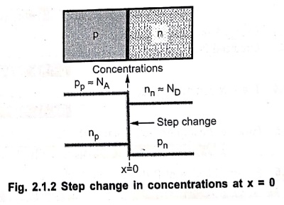
Fig. 2.1.2 Step change
in concentrations at x = 0
•
These changes in the carrier concentrations at the junction are shown in Fig.
2.1.2
•
It can be seen that at x = 0 i.e. at the junction, the changes in the
concentrations of carriers are sudden.
•
These sudden changes appear as the step type changes at the junction.
•
For the holes, there is a step change from Pp to Pn while for the electrons
there is a step change from np to nn, at x = 0.
•
Due to this, the p‒n junction is called step graded p‒n junction or abrupt p‒n
junction.
Key
Point: As the atomic characteristics of trivalent and
pentavalent impurity atoms differ from each other, the valence and conduction
bands on n side are at little bit lower energy levels than on P side.
Review
Questions
1. What is a p‒n junction?
2. Explain the basic structure of p‒n junction.
Electron Devices: Chapter 2: PN Junction Diodes : Tag: electronics : - Basic Structure of PN Junction
Electron Devices: Chapter 2: PN Junction Diodes
Under Subject

Electron Devices
EC25C01 2nd Semester ECE Dept | 2025 Regulation | 2nd Semester 2025 Regulation
Related Subjects

English Essentials II
EN25C02 2nd Semester | 2025 Regulation | 2nd Semester 2025 Regulation

Tamils and Technology தமிழர்களும் தொழில்நுட்பமும்
UC25H02 2nd Semester | 2025 Regulation | 2nd Semester 2025 Regulation

Linear Algebra
MA25C02 2nd Semester | 2025 Regulation
Electron Devices
EC25C01 2nd Semester ECE Dept | 2025 Regulation | 2nd Semester 2025 Regulation

Data Structures using CPlusPlus
CS25C05 2nd Semester ECE Dept | 2025 Regulation | 2nd Semester 2025 Regulation

Circuits and Network Analysis
EC25C02 2nd Semester ECE Dept | 2025 Regulation | 2nd Semester 2025 Regulation

Re-Engineering for Innovation
ME25C05 2nd Semester | 2025 Regulation | 2nd Semester 2025 Regulation

Engineering Drawing - Laboratory
ME25C01 2nd Semester | 2025 Regulation | 2nd Semester 2025 Regulation

Data Structures using CPlusPlus - Laboratory
CS25C05 2nd Semester ECE Dept | 2025 Regulation | 2nd Semester 2025 Regulation

Devices and Circuits Laboratory
EC25C03 2nd Semester ECE Dept | 2025 Regulation | 2nd Semester 2025 Regulation