Electron Devices: Chapter 2: PN Junction Diodes
PN Junction Diodes: Important Example Solved Problems
Electron Devices
Electron Devices: Chapter 2: PN Junction Diodes: Anna University Solved Problems, Assignment Problems and Important Solved Problems
Electron
Devices
Chapter 2: PN Junction
Diodes
Important
Part B Questions
Energy
Band Structure of Open Circuited P‒N Junction
Ex. 1: Consider a Si PN junction at T = 300° K with doping concentrations of NA =1016 cm‒3 and ND = 1015 cm-3. Assume that ni = 1.5×1010 cm-3. Calculate width of the space charge region in a PN junction, when a reverse bias voltage VR = 5 V is applied.
Solution:
T
= 300°K,
NA
=1016 /cm3, ND = 1015 / cm3,
ni =1.5×10¹⁰ /cm3,
VR = 5V, εr = 11.7 for Si,
q = 1.6×10‒19
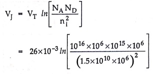
VJ
= VT In [NAND / ni2]
=
26×10‒3 In [ (1016×106×1015×106)
/ (1.5×1010×106)2 ]
=
0.637 V
VB
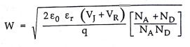
= VJ+VR = 5 + 0.637 = 5.637 V
=
2.833 μm
Note
that NA =1016/cm3 = 1016 × 106/m3
=1022/m3
Ex. 2: Calculate the built in
potential barrier in a PN junction. Consider a silicon PN junction at 300 °K
with doping densities NA =1×1018 cm-3 and ND
=1×1015 cm-3. Assume ni =1.5×10¹⁰
cm-3.
Solution:
T
= 300 °K, NA =1×10¹⁸ / cm3 = 1×1024
/m3,
ND
=1×10¹⁵ / cm3 =1×10²¹/m3, ni
ni =1×10¹⁵ / cm3 = 1×10²¹/m3
VT
= 0.0259 V at T = 300 °K
VJ
= VT In[NAND /ni2]
=
0.178 V
Diode
Current Equation and Nature of Characteristics
Ex: 3: The reverse saturation of a
silicon PN junction diode is 10 μA Calculate the diode current for the forward
bias voltage of 0.6 V at 25 °C.
Solution:
I0 = 10 μA, η = 2 for silicon, V =
0.6 V,
T = 25°C = 25+ 273 °K = 298 °K
VT
= kT = 8.62×10‒5×298 = 0.025 V
Using
diode current equation,
I
= I0 [eV/ηVT
‒1]
=
10×10‒6 [e0.6/2×0.025 −1] = 1.6275 A
Ex. 4: The voltage across a
silicon diode at room temperature of 300 °K is 0.71 V when 2.5 mA current flows
through it. If the voltage increases to 0.8 V, calculate the new diode current.
Solution:
The
current equation of a diode is
I
= I0 [eV/ηVT
‒1]
At
300 °K, VT = 26 mV = 26×10‒3 V
V = 0.71 V for I = 2.5 mA
and
η = 2 for silicon
2.5×10‒3
= I0 [e(0.71/2×26×10−3) ‒ 1]
i.e.,
I0 = 2.93 × 10‒9 V
Now
V = 0.8 V, I0 remains same.
I = 2.93 × 10‒9 [e(0.8/2×26×10‒3)
‒1]
= 0.0141 A = 14.11 mA
Ex. 5: A germanium diode has a
reverse saturation current of 3 μA. Calculate the voltage at which 1 % of the
rated current will flow through the diode, at room temperature if diode is
rated for 1 A.
Solution:
η = 1 for germanium, I0 = 3 μА = 3×10‒6
A
Rated
current is 1 A, and
I = 1 % of rated current = 0.01 A.
VT = 26 mV at room temperature
Using
current equation of a diode,
I = I0 [eV/ηVт − 1]
i.e.,
0.01= 3×10‒6 [eV/1×26×10−3 ‒ 1]
3333.33 = eV/1×26×10−3 ‒ 1
i.e.
eV/1×26×10‒3 = 3334.33
V
/ 26×10‒3 = 8.112
i.e.
V = 0.2109 V
Ex.6: The diode current is 0.6 mA
when the applied voltage is 400 mV and 20 mA when the applied voltage is 500
mV. Determine η. Assume kT/q = 25mV.
Solution:
At
V1 = 400 mV, I1 = 0.6 mA
V2
= 500 mV, I2 = 20 mA,
VT
= 25 mV (given)
I
= I0 [eV/ηVт −
1]
….. Diode current equation
0.6×10‒3 = I0 [e400×10‒3/η×25×10‒3
‒ 1]
……….. (1)
20×10‒3 = I0 [e500×10‒3/η×25×10−3
‒ 1]
………..(2)
In
forward biased condition, 1 <<< eV/ηVT
so neglecting 1,
0.6×10‒3 = I0 e16/η
and
20×10‒3 = 10 e20/η
Dividing
the two equations,
0.6
/ 20 = e16/η / e20/η
e16/η
= 0.03 e20/η
Taking
natural logarithm of both sides,
16/η = In 0.03 + 20/η
i.e.
1/η(16‒20) = ‒ 3.50655
1/η
= 0.87664
i.e.
n = 1.1407
Solving
equation (1)
I0
= 4.8598 × 10‒10 A
Derivation
of V‒I Characteristics of P‒N Junction Diode (Diode Current Equation)
Ex. 7: Determine the ideal reverse
saturation current density in a silicon pn junction at T = 300 °K. Consider the
following parameters in the silicon pn junction: NA = ND
= 1016 cm3, ni = 1.5×1010 cm-3,
Dn =25 cm2/s. τp0 = τn0 =5×10‒7
s, Dp = 10 cm2 / s, εr = 117. Comment on the
result.
Solution:
The
reverse current density is given by,
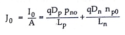
The
diffusion length for the holes and electrons is given by,
Lp = √(Dpτp)
Ln = √(Dnτn)
np0 = ni2
/ NA
Pno = ni2
/ ND
….. by law of mass action
Lp = √(Dpτp)
= √[10×10‒4×5×10‒7] = 2.236×10‒5
Ln = √(Dnτn)
= √[25×10‒4×5×10‒7] = 3.535×10‒5
np0 = ni2
/ NA = (1.5×10¹⁶)2 /
1022 =2.25×10¹⁰
Pno = ni2
/ ND= (1.5×10¹⁶)2 / 1022
=2.25×10¹⁰
q
= 16×10‒19 C and using in (1),
J0
= 1.6×10‒19 [ (10×10‒4×2.25×1010 / 2.236×10‒5
) + (25×10-4×2.25×1010 /3.535×10‒5) ]
= 4.15×10‒7A/m2
i.e.4.15×10‒11
A/cm2
Mathematical
Expression for the Dynamic Resistance
Ex. 8: A p‒n junction diode has at
a temperature of 125°C a reverse saturation current of 30 μ A. At a temperature
of 125°C find the dynamic resistance for 0.2 V bias in forward and reverse
direction.
Solution:
Now
T
= 125 °C, V = ± 0.2 V, I0 = 30 μА
VT
= kT at temperature T in °K
T=
125 + 273 = 398 °K
and
k = 8.62×10‒5 = Boltzmann's constant
and
VT
= 398×8.62×10‒5
= 0.034307 V = 34.3076 mV
The
dynamic resistance is given by,
r = ηVT / I0eV/ηVT
Assume
germanium diode, η = 1
For
forward bias, V = +0.2 V
rf = ( 1×0.0343076 ) / ( 30×10‒6
× e0.2/0.0343076 )
= 3.3612 Ω
For
reverse bias, V = ‒ 0.2 V
rr = ( 1×0.0343076 ) / ( 30×10‒6
×e‒0.2/0.0343076 )
= 389.078 ΚΩ
Effect of
Temperature on Diode Behaviour
Ex. 9: The reverse saturation
current of a silicon diode is 5 mA at room temperature. Find the diode current
at i) 40 °C and a forward voltage of 0.3 V. ii) 60 °C and a forward voltage of
0.5 V.
Solution:
I01 = 5 mA at room temperature of T1
= 27 °C = 300 °K
i)
At T2 = 40 °C = 40+ 273 = 313 °K and V = 0.3 V
ΔT
= T2‒T1 = 313‒300 = 13
(I02)
= (2ΔT/10) I01
=
(213/10) × 5 × 10-3
=
12.3114 mA
η = 2 for silicon
VT
= T2 / 11600 = 313 / 11600
=
0.02698 A
I
= I02 [eV/ηVT
‒1]
=
12.3114 [e0.3/2×0.02698 ‒1]
=
3185.428 mA = 3.185 A
i)
At T3 = 60 °C = 333 °K and V
= 0.5 V
ΔT
= T3‒T1 = 333‒300 = 13
(I03)
= (2ΔT/10) I01
=
(233/10) × 5 × 10-3
=
49.2457 mA
VT
= T3 / 11600 = 333 / 11600
=
0.0287 A
I
= I03 [eV/ηVT
‒1]
=
49.2457 [e0.5/2×0.0287 ‒1]
=
298778.75 mA
=
298.7787 A
Ex. 10: The reverse saturation current
of a germanium diode is 100 μA at room temperature of 27 °C. Calculate the
current in forward biased condition, if forward bias voltage is 0.2 V at room
temperature. If temperature is increased by 20 °C, calculate the reverse
saturation current and the forward current, for same current and the forward
voltage, at new temperature.
Solution:
At
T1 = 27 °C = 300 °K, VT = 26 mV
(I0)1 = 100 μA,
V
= 0.2 V
I
= I0 [eV/ηVT
‒1]
=
100×10‒6 [e0.2/1×26×10−3 −1]
=
219.04 mA
Using
the approximate result,
(I0)2 = 2T2‒T1 /
10] ×(I0)1
=
2(20/10) ×(I0)1
…… T2‒T1 =20°C
=
4×100 = 400 μА
New
reverse current at 27 + 20 = 47°C is 400 μA. So for V = 0.2 V, the new forward
current can be calculated using current equation of diode.
VT
at T2 = 47 + 273 = 320 °K = KT
=
8.62×10‒5×320 = 27.584 mV
I
= I0 [eV/ηVT
‒1]
=
400 × 10‒6 [e0.2/1×27.584 × 10−3 ‒ 1 ]
=
563.158 mA
Transition
Capacitance (CT)
Ex. 11: A germanium diode has a
contact potential of 0.2 V and concentration of acceptor impurity is 3×10²⁰/m3.
Area of cross‒section of junction is 1 mm2 and εr = 16.
Calculate width of depletion region and transition capacitance for reverse bias
of a) 0.1 V and b) 10 V (Assume charge on each electron as 1.6 × 10‒19C)
Solution:
V1 = 0.2 V, NA = 3 × 10²⁰/m3,
A = 1 mm2, εr = 16
a)
V = ‒0.1 V
……… Negative as reverse bias
VB = VJ‒ V = 0.2 − (−
0.1) = 0.3 V
VB = qNA/ε . W2/2
i.e.
0.3 = (1.6 × 10‒19 × 3 × 1020)
/ (8.854 × 10‒12 × 16) . W2/2
W = 1.33 μm,
Ст = εA/W = (ε×1×10‒19)
/ (1.33×10‒6) = 106.45 pF
b)
V = ‒10V
hence
VB
= VJ ‒ V = 0.2 ‒ (‒10) = 10.2 V
10.2 = [ 1.6 × 10‒19 × 3 × 1020
] / [8.854 × 10‒12 × 16] × [W2/2]
i.e.
W
= 7.75 μm
Ст
= εA
=
( 8854 × 10‒12 × 16 × 1 × 10‒6 ) / (7.75 × 10‒6)
=
18.25 pF
Thus
as reverse bias voltage increases, width of depletion region increases while
transition capacitance decreases.
Electron Devices: Chapter 2: PN Junction Diodes : Tag: electronics : Electron Devices - PN Junction Diodes: Important Example Solved Problems
Electron Devices: Chapter 2: PN Junction Diodes
Under Subject

Electron Devices
EC25C01 2nd Semester ECE Dept | 2025 Regulation | 2nd Semester 2025 Regulation
Related Subjects

English Essentials II
EN25C02 2nd Semester | 2025 Regulation | 2nd Semester 2025 Regulation

Tamils and Technology தமிழர்களும் தொழில்நுட்பமும்
UC25H02 2nd Semester | 2025 Regulation | 2nd Semester 2025 Regulation

Linear Algebra
MA25C02 2nd Semester | 2025 Regulation
Electron Devices
EC25C01 2nd Semester ECE Dept | 2025 Regulation | 2nd Semester 2025 Regulation

Data Structures using CPlusPlus
CS25C05 2nd Semester ECE Dept | 2025 Regulation | 2nd Semester 2025 Regulation

Circuits and Network Analysis
EC25C02 2nd Semester ECE Dept | 2025 Regulation | 2nd Semester 2025 Regulation

Re-Engineering for Innovation
ME25C05 2nd Semester | 2025 Regulation | 2nd Semester 2025 Regulation

Engineering Drawing - Laboratory
ME25C01 2nd Semester | 2025 Regulation | 2nd Semester 2025 Regulation

Data Structures using CPlusPlus - Laboratory
CS25C05 2nd Semester ECE Dept | 2025 Regulation | 2nd Semester 2025 Regulation

Devices and Circuits Laboratory
EC25C03 2nd Semester ECE Dept | 2025 Regulation | 2nd Semester 2025 Regulation