Electron Devices: Chapter 2: PN Junction Diodes
Forward Biasing of PN Junction Diode

Questions: 1. With a neat diagram explain the working of a PN junction diode in forward bias condition. 2. Explain the static and dynamic resistances of the diodes. 3. Explain the V‒I characteristics of diode in forward biased mode. 4. With necessary diagram, describe the characteristics of a forward biased PN junction diode. Index; 1. Operation of Forward Biased Diode 2. Effect on the Depletion Region 3. Effect of the Barrier Potential 4. Forward VI Characteristics of Diode 5. Forward Resistance of Diode
Forward
Biasing of P‒N Junction Diode
•
If an external d.c. voltage is connected in such a way that the p‒region
terminal is connected to the positive of the d.c. voltage and the n‒region is
connected to the negative of the d.c. voltage, the biasing condition is called
forward biasing. The p‒n junction is said to be forward biased.
•
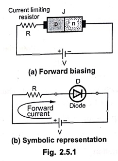
Fig. 2.5.1 (a) shows the connection of forward biasing of a p‒n junction.
•
To limit the current, practically a current limiting resistor is connected in
series with the p‒n junction diode.
•
Fig. 2.5.1 (b) shows the symbolic representation of a forward biased diode.
1. Operation of Forward Biased Diode
•
When the p‒n junction is forward biased as long as the applied voltage is less
than the barrier potential, there cannot be any conduction.
•
When the applied voltage becomes more than the barrier potential, the negative
terminal of battery pushes the free electrons against barrier potential from n
to p‒region.
•
Similarly positive terminal pushes the holes from p to n‒region. Thus holes get
repelled by positive terminal and cross the junction against barrier potential.
•
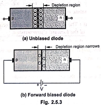
Thus the applied voltage overcomes the barrier potential. This reduces the
width of depletion region.
•
As forward voltage is increased, at a particular value the depletion region
becomes very much narrow such that large number of majority charge carriers can
cross the junction.
•
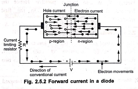
The large number of majority carriers constitute a current called forward
current.
•
The current in the p‒region is the movement of holes which are majority
carriers. This is the hole current. While the current in the n‒region is the
movement of free electrons which are majority carriers. This is the electron
current.
•
Hence the overall forward current is due to the majority charge carriers. The
action is shown in Fig. 2.5.2.
•
These majority carriers can then travel around the closed circuit and a
relatively large current flows.
2. Effect on the Depletion Region
•
Due to the forward bias voltage, more electrons flow into the depletion region,
which reduces the number of positive ions. Similarly flow of holes reduces the
number of negative ions.
•
This reduces the width of the depletion region. This is shown in Fig. 2.5.3.
Key
Point: Depletion region narrows due to forward bias
voltage.
3. Effect of the Barrier Potential
•
Under the influence of applied forward bias voltage, the free electrons get the
energy equivalent to the barrier potential so that they can easily overcome the
barrier, which is a sort of a hill and cross the junction.
•
While crossing the junction, the electrons give up the amount of energy
equivalent to the barrier potential.
•
This loss of energy produces a voltage drop across the p‒n junction which is
almost equal to the barrier potential.
Key
Point: The polarities of voltage drop across the p‒n
junction in forward biased condition are opposite to that of barrier potential
but the value is almost equal to the barrier potential.
•
Due to the internal resistance, there is additional small voltage drop across
the diode.
•
Thus the total voltage drop across a p‒n junction diode in a forward biased
condition is Vf and it is made up of,
1.
Drop due to barrier potential and
2.
Drop due to internal resistance.
Vf
= Vγ + If rf
Key
Point: The total Vf is of the order of 0.7 V
for silicon and 0.3 V for the germanium.
4. Forward VI Characteristics of Diode
•
The response of p‒n junction can be easily indicated with the help of
characteristics called V-I characteristics of p‒n junction.
•
It is the graph of voltage applied across the p‒n junction and the current
flowing through the p‒n junction.
•
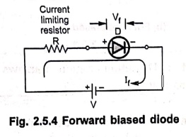
Fig. 2.5.4 shows the forward biased diode.
•
The applied voltage is V while the voltage across the diode is Vf.
•
The current flowing in the circuit is the forward current If.
•
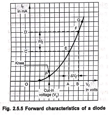
The graph of forward current If against the forward voltage Vf
across the diode is called forward characteristics of a diode.
•
The forward characteristics of a diode is shown in Fig. 2.5.5.
•
Basically forward characteristics can be divided into two regions:
1. Region O to P:
As long as Vf is less than cut‒in voltage (Vγ), the
current flowing is very small. Practically this current is assumed to be zero.
2. Region P to Q and
onwards: As Vf increases towards Vγ
the width of depletion region goes on reducing. When Vf exceeds Vγ
i.e. cut‒in voltage, the depletion region becomes very thin and current If
increases suddenly. This increase in the current is exponential as shown in
Fig. 2.5.5 by the region P to Q.
•
The point P, after which the forward current starts increasing exponentially is
called knee of the curve and the corresponding voltage is called knee voltage.
Key
Point: The normal forward biased operation of the diode is
above the knee point of the curve. i.e. in the region P‒Q.
•
The forward current is the conventional current, hence it is treated as
positive and the forward voltage Vf is also treated positive. Hence
the forward characteristics is plotted in the first quadrant.
5. Forward Resistance of Diode
•
The resistance offered by the p‒n junction diode in forward biased condition is
called forward resistance. The forward resistance is defined in two ways:
1) Static forward
resistance : This is the forward resistance of p‒n
junction diode when p‒n junction is used in d.c. circuit and the applied
forward voltage is d.c. This resistance is denoted as Rf and is
calculated at a particular point on the forward characteristics.
Rf = Forward
d.c. voltage / Forward d. c. current
= ОА / OC at point E
2) Dynamic forward
resistance: The resistance offered by the p‒n
junction under a.c. conditions is called dynamic resistance denoted as rf.
Key
Point: The dynamic resistance is reciprocal of the slope
of the forward characteristics.
•
Consider the change in applied voltage from point A to B shown in Fig. 2.5.5.
This is denoted as ΔVf.
•
The corresponding change in the forward current is from point C to D. It is
denoted as ΔIf.
•
Thus the slope of the characteristics is ΔIf/ΔVf. The
reciprocal of the slope is dynamic resistance rf.
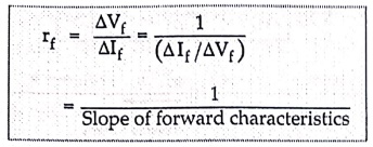
rf = ΔVf / ΔIf = 1 / (ΔIf / ΔVf)
= 1 / Slope of forward characteristics
Key
Point: Generally the value of rf is very small of
the order of few ohms, in the operating region i.e. above the knee.
Review
Questions
1. With a neat diagram explain the working of a PN junction
diode in forward bias condition.
2. Explain the static and dynamic resistances of the diodes.
3. Explain the V‒I characteristics of diode in forward biased
mode.
4. With necessary diagram, describe the characteristics of a forward
biased PN junction diode.
Electron Devices: Chapter 2: PN Junction Diodes : Tag: electronics : - Forward Biasing of PN Junction Diode
Electron Devices: Chapter 2: PN Junction Diodes
Under Subject

Electron Devices
EC25C01 2nd Semester ECE Dept | 2025 Regulation | 2nd Semester 2025 Regulation
Related Subjects

English Essentials II
EN25C02 2nd Semester | 2025 Regulation | 2nd Semester 2025 Regulation

Tamils and Technology தமிழர்களும் தொழில்நுட்பமும்
UC25H02 2nd Semester | 2025 Regulation | 2nd Semester 2025 Regulation

Linear Algebra
MA25C02 2nd Semester | 2025 Regulation
Electron Devices
EC25C01 2nd Semester ECE Dept | 2025 Regulation | 2nd Semester 2025 Regulation

Data Structures using CPlusPlus
CS25C05 2nd Semester ECE Dept | 2025 Regulation | 2nd Semester 2025 Regulation

Circuits and Network Analysis
EC25C02 2nd Semester ECE Dept | 2025 Regulation | 2nd Semester 2025 Regulation

Re-Engineering for Innovation
ME25C05 2nd Semester | 2025 Regulation | 2nd Semester 2025 Regulation

Engineering Drawing - Laboratory
ME25C01 2nd Semester | 2025 Regulation | 2nd Semester 2025 Regulation

Data Structures using CPlusPlus - Laboratory
CS25C05 2nd Semester ECE Dept | 2025 Regulation | 2nd Semester 2025 Regulation

Devices and Circuits Laboratory
EC25C03 2nd Semester ECE Dept | 2025 Regulation | 2nd Semester 2025 Regulation