Electron Devices: Chapter 2: PN Junction Diodes
Complete VI Characteristics of a PN Junction Diode
Questions: 1. Draw and explain the V‒I characteristics of a PN junction diode. 2. Draw and compare V‒I characteristics of typical Ge and Si diodes.
Complete
V‒I Characteristics of a Diode
•
The complete V‒I characteristics of a diode is the combination of its forward
as well as reverse characteristics. This is shown in Fig. 2.7.1.
•
In forward characteristics, it is seen that initially forward current is small
as long as the bias voltage is less than the barrier potential. At a certain
voltage close to barrier potential, current increases rapidly.
•
The voltage at which diode current starts increasing rapidly is called as cut‒in
voltage. It is denoted by Vγ.
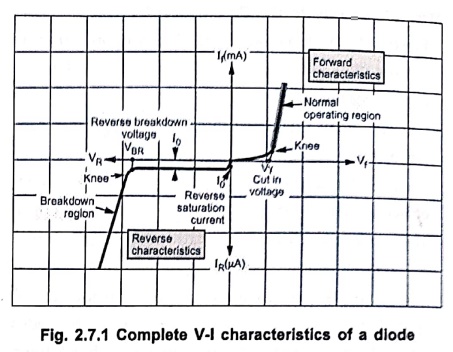
Fig. 2.7.1 Complete V‒I
characteristics of a diode
•
Below this voltage, current is less than 1% of maximum rated value of diode
current. The cut‒in voltage for germanium is about 0.2 V while for silicon it
is 0.6 V.
•
It is important to note that the breakdown voltage is much higher and
practically diodes are not operated in the breakdown condition.
•
The voltage at which breakdown occurs is called reverse breakdown voltage
denoted as VBR.
Key
Point: Reverse current before the breakdown is very very
small and can be practically neglected.
V‒I Characteristics of Typical Ge and Si Diodes
•
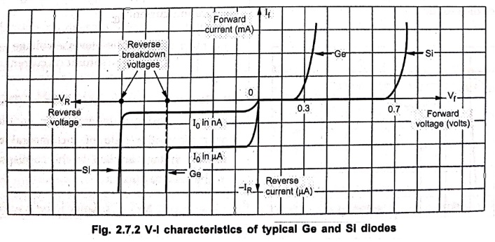
The potential for Germanium (Ge) diode is about 0.3 V while for Silicon (Si)
diode is as about 0.7 V.
•
The potential at which current starts increasing exponentially is also called
Offset potential, Threshold potential or Firing potential of a diode.
• Fig. 2.7.2 shows the V‒I characteristics of typical Ge and Si diodes.
•
The reverse saturation current in a germanium diode is about 1000 times more
than the reverse saturation current in a silicon diode of a comparable rating.
The reverse saturation current I0 is of the order of nA for silicon
diode while it is of the order of μA for germanium diode.
•
Reverse breakdown voltage for Si diode is higher than that of the Ge diode of a
comparable rating.
Review Questions
1. Draw and explain the V‒I characteristics of a PN junction
diode.
2. Draw and compare V‒I characteristics of typical Ge and Si
diodes.
Electron Devices: Chapter 2: PN Junction Diodes : Tag: electronics : - Complete VI Characteristics of a PN Junction Diode
Electron Devices: Chapter 2: PN Junction Diodes
Under Subject

Electron Devices
EC25C01 2nd Semester ECE Dept | 2025 Regulation | 2nd Semester 2025 Regulation
Related Subjects

English Essentials II
EN25C02 2nd Semester | 2025 Regulation | 2nd Semester 2025 Regulation

Tamils and Technology தமிழர்களும் தொழில்நுட்பமும்
UC25H02 2nd Semester | 2025 Regulation | 2nd Semester 2025 Regulation

Linear Algebra
MA25C02 2nd Semester | 2025 Regulation
Electron Devices
EC25C01 2nd Semester ECE Dept | 2025 Regulation | 2nd Semester 2025 Regulation

Data Structures using CPlusPlus
CS25C05 2nd Semester ECE Dept | 2025 Regulation | 2nd Semester 2025 Regulation

Circuits and Network Analysis
EC25C02 2nd Semester ECE Dept | 2025 Regulation | 2nd Semester 2025 Regulation

Re-Engineering for Innovation
ME25C05 2nd Semester | 2025 Regulation | 2nd Semester 2025 Regulation

Engineering Drawing - Laboratory
ME25C01 2nd Semester | 2025 Regulation | 2nd Semester 2025 Regulation

Data Structures using CPlusPlus - Laboratory
CS25C05 2nd Semester ECE Dept | 2025 Regulation | 2nd Semester 2025 Regulation

Devices and Circuits Laboratory
EC25C03 2nd Semester ECE Dept | 2025 Regulation | 2nd Semester 2025 Regulation