Electron Devices: Chapter 2: PN Junction Diodes
Switching Characteristics of PN Junction Diode
Questions: 1. Explain the switching characteristics of diode with the help of simple diode circuit. 2. Write short notes on diode switching characteristics.
Switching
Characteristics of Diode
•
When the diode is switched from forward biased to reverse biased or viceversa,
it takes finite time to reach the final steady state. The behaviour of diode
during this time is called switching characteristics of diode.
•
To study the switching characteristics of diode consider simple diode circuit
and an input waveform as shown in Fig. 2.15.1.
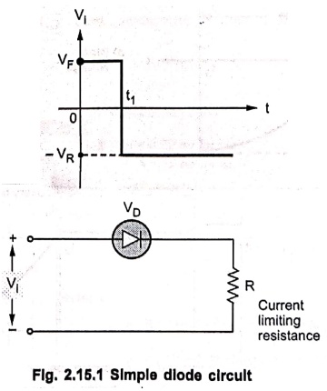
The
following events will take place due to the nature of the applied voltage.
•
Event 1: Till time t1,
the forward voltage applied is VF and diode is forward biased. The
value of R is large enough such that drop across forward biased diode is very
small compared to drop across R. The forward current is then IF ≈ VF/R,
neglecting forward resistance of diode.
•
Event 2: At time t1,
the applied voltage is suddenly reversed and reverse voltage of ‒VR
is applied to the circuit. Ideally diode also must become OFF from ON state
instantly. But this does not happen instantly. The number of minority carriers
take time to reduce from Pn ‒Pno to zero at the junction
as shown in Fig. 2.15.2 (b). Due to this, at tı current just reverses and
remains at that reversed value ‒IR till the minority carrier
concentration reduces to zero. This current is given by ‒IR = ‒VR
/ R. This continues to flow till time t2.
Key Point:
During time t1 to t2, the minority charge carriers remain
stored and decrease slowly to zero. Hence this time is called storage time
denoted as ts.
•
Event 3 : From t2
onwards, the diode voltage starts to reverse and the diode current starts
decreasing as shown in Fig. 2.15.2 (c). At t=t3; the diode state
completely gets reversed and attains steady state in reverse biased condition.
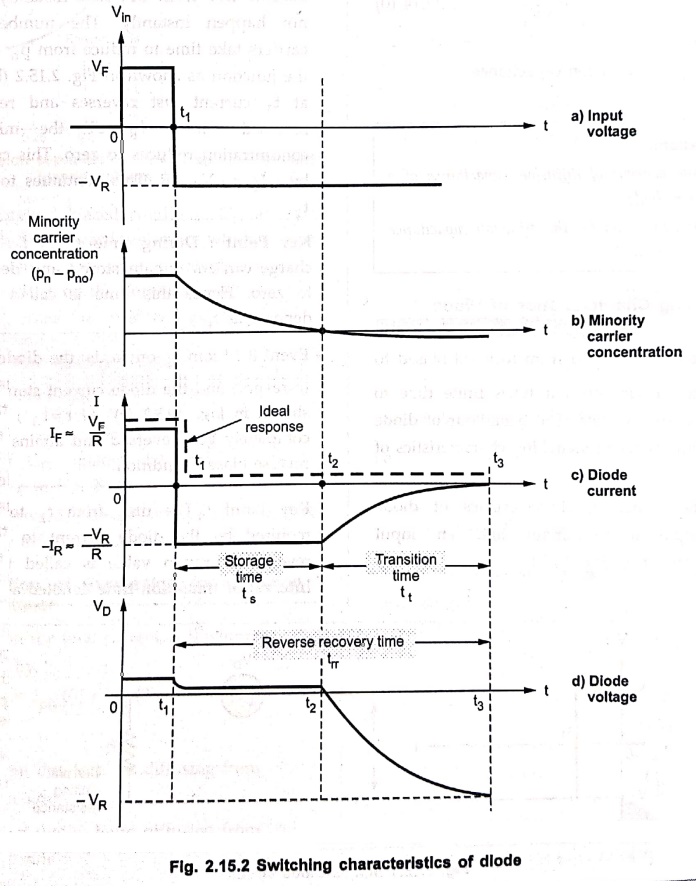
Key Point: The time from t2 to t3 i.e. time required by the diode current to reduce to its reverse saturation value is called the transition interval or transition time denoted as tt.
•
The total time required by the diode which is the sum of storage time and
transition time, to recover completely from the change of state is called
reverse recovery time of the diode and denoted as trr. This is an
important consideration in high speed switching applications.
Key
Point: For quick switching from ON to OFF state, the
reverse recovery time should be as small as practicable.
trr = ts + tt .. (2.15.1)
•
The reverse recovery time depends on the RC time constant where C is a
transition capacitance of a diode.
Key
Point: To have fast switching from ON to OFF of a diode,
the transition capacitance should be as small as possible.
• Thus the transition capacitance plays an important role in the switching circuits using diodes.
•
Most commercially available switching diodes have the reverse recovery time
ranging from a few nanoseconds to one microsecond. However, diodes are
specially manufactured having reverse recovery time as small as only a few
picoseconds.
•
The total switching time trr puts the limit on the maximum operating
frequency of the diode. Hence trr is an important datasheet
specification. To minimize the effect of the reverse current, the time period
of the operating frequency must be atleast ten times trr.
T
= 10 trr
fmax = 1 / T = 1 / 10trr
•
where fmax is the maximum operating frequency.
Review
Questions
1. Explain the switching characteristics of diode with the help
of simple diode circuit.
2. Write short notes on diode switching characteristics.
Electron Devices: Chapter 2: PN Junction Diodes : Tag: electronics : - Switching Characteristics of PN Junction Diode
Electron Devices: Chapter 2: PN Junction Diodes
Under Subject

Electron Devices
EC25C01 2nd Semester ECE Dept | 2025 Regulation | 2nd Semester 2025 Regulation
Related Subjects

English Essentials II
EN25C02 2nd Semester | 2025 Regulation | 2nd Semester 2025 Regulation

Tamils and Technology தமிழர்களும் தொழில்நுட்பமும்
UC25H02 2nd Semester | 2025 Regulation | 2nd Semester 2025 Regulation

Linear Algebra
MA25C02 2nd Semester | 2025 Regulation
Electron Devices
EC25C01 2nd Semester ECE Dept | 2025 Regulation | 2nd Semester 2025 Regulation

Data Structures using CPlusPlus
CS25C05 2nd Semester ECE Dept | 2025 Regulation | 2nd Semester 2025 Regulation

Circuits and Network Analysis
EC25C02 2nd Semester ECE Dept | 2025 Regulation | 2nd Semester 2025 Regulation

Re-Engineering for Innovation
ME25C05 2nd Semester | 2025 Regulation | 2nd Semester 2025 Regulation

Engineering Drawing - Laboratory
ME25C01 2nd Semester | 2025 Regulation | 2nd Semester 2025 Regulation

Data Structures using CPlusPlus - Laboratory
CS25C05 2nd Semester ECE Dept | 2025 Regulation | 2nd Semester 2025 Regulation

Devices and Circuits Laboratory
EC25C03 2nd Semester ECE Dept | 2025 Regulation | 2nd Semester 2025 Regulation