Electron Devices: Chapter 2: PN Junction Diodes
PN Junction Diode Current Equation and Nature of Characteristics
Questions: 1. Write the diode current equation of a p‒n junction and explain the V‒I characteristics from it. 2. Important Example Solved Problems 3. Explain the theory of PN junction diode and derive its diode current equation.
Diode
Current Equation and Nature of Characteristics
•
The relationship between applied voltage V and the diode current I is
exponential and is mathematically (given by the equation called diode current
equation. It is expressed as,
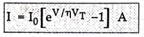
I = I0
[eV/ηVT ‒1] A
where
I0 = Reverse saturation current in
amperes,
V
= Applied voltage
η = 1 for germanium diode
and = 2 for silicon diode
VT = Voltage equivalent of
temperature in volts
•
The voltage equivalent of temperature indicates dependence of diode current on
temperature.
•
The voltage equivalent of temperature VT for a given diode at
temperature T is calculated as,
VT
= KT volts
where
k = Boltzmann's constant = 8.62×10⁻⁵eV/°K
and
T = Temperature in °K.
•
Thus at room temperature of 27 °C i.e. T = 27+ 273 = 300°K the value of VT
is,
VT
= 8.62 × 10‒5 × 300 = 0.02586 V ≈ 26 mV
•
The diode current equation is applicable for all the conditions of diode i.e.
unbiased, forward biased and reverse biased.
For
forward biased, V must be taken positive and we get current I positive which is
forward current. For reverse biased, V must be taken negative and we get
negative current I which indicates that it is reverse current.
1. Nature of V‒I Characteristics from Equation of Diode
•
Consider a current equation of diode as,
I = I0(eV/ηVT −1)
•
Now for a forward biased condition, the bias voltage V is considered positive
and hence exponential index has positive sign. Due to this, 1 <<< eV/ηVT
hence neglecting 1 we get the equation for a forward current as,
If
= I0eV/ηVT
•
This indicates that once bias voltage exceeds cut‒in voltage, the forward
current increases exponentially. In reverse biased condition, the bias voltage
V is treated negative and due to this exponential index has negative sign. So e‒V/ηVT
<< 1, hence neglecting exponential term we get,
αIR
≡ I0(−1) ≡ – I0
•
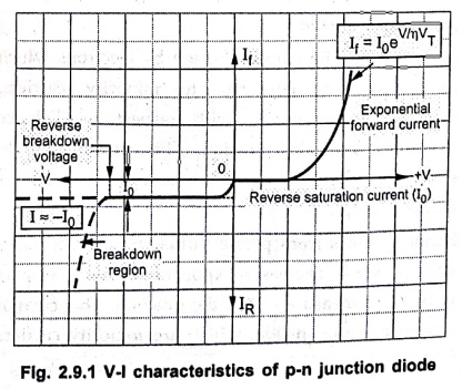
The above equation indicates that under reverse biased condition, the current
is reverse saturation current which is negative indicating that it flows in
opposite direction to that of forward current and almost constant.
•
Such nature of diode characteristics is already been discussed and it is as
shown in Fig. 2.9.1. The dashed portion represents breakdown region.
Ex: 2.9.1: The reverse saturation of a
silicon PN junction diode is 10 μA Calculate the diode current for the forward
bias voltage of 0.6 V at 25 °C.
Solution:
I0 = 10 μA, η = 2 for silicon, V =
0.6 V,
T = 25°C = 25+ 273 °K = 298 °K
VT
= kT = 8.62×10‒5×298 = 0.025 V
Using
diode current equation,
I
= I0 [eV/ηVT
‒1]
=
10×10‒6 [e0.6/2×0.025 −1] = 1.6275 A
Ex. 2.9.2: The voltage across a silicon
diode at room temperature of 300 °K is 0.71 V when 2.5 mA current flows through
it. If the voltage increases to 0.8 V, calculate the new diode current.
Solution:
The
current equation of a diode is
I
= I0 [eV/ηVT
‒1]
At
300 °K, VT = 26 mV = 26×10‒3 V
V = 0.71 V for I = 2.5 mA
and
η = 2 for silicon
2.5×10‒3
= I0 [e(0.71/2×26×10−3) ‒ 1]
i.e.,
I0 = 2.93 × 10‒9 V
Now
V = 0.8 V, I0 remains same.
I = 2.93 × 10‒9 [e(0.8/2×26×10‒3)
‒1]
= 0.0141 A = 14.11 mA
Ex. 2.9.3: A germanium diode has a reverse
saturation current of 3 μA. Calculate the voltage at which 1 % of the rated
current will flow through the diode, at room temperature if diode is rated for
1 A.
Solution:
η = 1 for germanium, I0 = 3 μА = 3×10‒6
A
Rated
current is 1 A, and
I = 1 % of rated current = 0.01 A.
VT = 26 mV at room temperature
Using
current equation of a diode,
I = I0 [eV/ηVт − 1]
i.e.,
0.01= 3×10‒6 [eV/1×26×10−3 ‒ 1]
3333.33 = eV/1×26×10−3 ‒ 1
i.e.
eV/1×26×10‒3 = 3334.33
V
/ 26×10‒3 = 8.112
i.e.
V = 0.2109 V
Ex.2.9.4: The diode current is 0.6 mA when
the applied voltage is 400 mV and 20 mA when the applied voltage is 500 mV.
Determine η. Assume kT/q = 25mV.
Solution:
At
V1 = 400 mV, I1 = 0.6 mA
V2
= 500 mV, I2 = 20 mA,
VT
= 25 mV (given)
I
= I0 [eV/ηVт −
1]
….. Diode current equation
0.6×10‒3 = I0 [e400×10‒3/η×25×10‒3
‒ 1]
……….. (1)
20×10‒3 = I0 [e500×10‒3/η×25×10−3
‒ 1]
………..(2)
In
forward biased condition, 1 <<< eV/ηVT
so neglecting 1,
0.6×10‒3 = I0 e16/η
and
20×10‒3 = 10 e20/η
Dividing
the two equations,
0.6
/ 20 = e16/η / e20/η
e16/η
= 0.03 e20/η
Taking
natural logarithm of both sides,
16/η = In 0.03 + 20/η
i.e.
1/η(16‒20) = ‒ 3.50655
1/η
= 0.87664
i.e.
n = 1.1407
Solving
equation (1)
I0
= 4.8598 × 10‒10 A
Review
Questions
1. Write the diode current equation of a p‒n junction and
explain the V‒I characteristics from it.
2. The current of germanium diode is 100 μA at a voltage of ‒1
V, at room temperature. Determine the magnitude of the current for the voltages
of ± 0.2 V at room temperature.
[Ans.:
291 mA, 99.95 μA ]
3. A silicon diode has a reverse saturation current of 60 nA.
Calculate the voltage at which 1 % of the rated current will flow through the
diode, at room temperature if diode is rated for 1 A. [Ans. : 0.6252 V]
4. Explain the theory of PN junction diode and derive its diode
current equation.
Electron Devices: Chapter 2: PN Junction Diodes : Tag: electronics : - PN Junction Diode Current Equation and Nature of Characteristics
Electron Devices: Chapter 2: PN Junction Diodes
Under Subject

Electron Devices
EC25C01 2nd Semester ECE Dept | 2025 Regulation | 2nd Semester 2025 Regulation
Related Subjects

English Essentials II
EN25C02 2nd Semester | 2025 Regulation | 2nd Semester 2025 Regulation

Tamils and Technology தமிழர்களும் தொழில்நுட்பமும்
UC25H02 2nd Semester | 2025 Regulation | 2nd Semester 2025 Regulation

Linear Algebra
MA25C02 2nd Semester | 2025 Regulation
Electron Devices
EC25C01 2nd Semester ECE Dept | 2025 Regulation | 2nd Semester 2025 Regulation

Data Structures using CPlusPlus
CS25C05 2nd Semester ECE Dept | 2025 Regulation | 2nd Semester 2025 Regulation

Circuits and Network Analysis
EC25C02 2nd Semester ECE Dept | 2025 Regulation | 2nd Semester 2025 Regulation

Re-Engineering for Innovation
ME25C05 2nd Semester | 2025 Regulation | 2nd Semester 2025 Regulation

Engineering Drawing - Laboratory
ME25C01 2nd Semester | 2025 Regulation | 2nd Semester 2025 Regulation

Data Structures using CPlusPlus - Laboratory
CS25C05 2nd Semester ECE Dept | 2025 Regulation | 2nd Semester 2025 Regulation

Devices and Circuits Laboratory
EC25C03 2nd Semester ECE Dept | 2025 Regulation | 2nd Semester 2025 Regulation