Electron Devices: Chapter 2: PN Junction Diodes
PN Junction Diodes: Two Marks Important Questions and Answers
Electron Devices
Electron Devices: Chapter 2: Anna University Part A Two Marks Important Questions and Answers
Electron
Devices
Chapter 2: PN Junction
Diodes
Two Marks
Questions with Answers
1. What is peak inverse
voltage?
In
reverse biased, opposite polarity voltage across diode. The maximum reverse
appears voltage which diode can withstand without breakdown is called peak
inverse voltage.
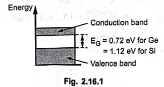
2. Draw the energy band
structure of Silicon and Germanium at room temperature indicating the energy
gap (EG) value in eV.
The
energy band structure is shown in Fig. 2.16.1.
3. What is meant by zener
breakdown?
When
a p‒n junction is heavily doped the depletion region is very narrow. So under
reverse bias conditions, the electric field across the depletion layer is very
intense. Electric field is voltage per distance and due to narrow depletion
region and high reverse voltage, it is intense. Such an intense field is enough
to pull the electrons out of the valence bands of the stable atoms. Such a
creation of free electrons is called zener effect. These minority carriers
constitute very large current to cause the breakdown and the mechanism is
called zener breakdown.
4. Compare the Silicon and Germanium diodes with
respect to cut‒in voltage and reverse saturation current.
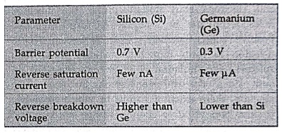
Barrier potential:
Silicon
(Si): 0.7 V
Germanium
(Ge): 0.3 V
Reverse saturation
Current:
Silicon
(Si): Few nA
Germanium
(Ge): Few μA
Reverse breakdown
voltage:
Silicon
(Si): Higher than Ge
Germanium
(Ge): Lower than Si
5. Define barrier potential
at the junction.
Due
to immobile positive charges on n side and negative charges on p side, there
exists an electric field across the unbiased p‒n junction. This creates
potential difference across the junction which is called a barrier potential.
Thus the voltage existing across the depletion region or barrier is called a
barrier potential.
6. Give the diode current
equation.
The
diode current equation is,
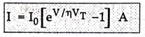
I = I0[eV/ηVT‒1] A
where
I0 = Reverse saturation current in
amperes
V = Applied voltage,
VT = Voltage equivalent of
temperature in volts
η = 1 for germanium diode and 2 for silicon diode
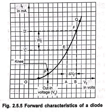
7. Define Knee voltage or a
cut‒in voltage of a diode.
When
diode is forward biased, some voltage is necessary to overcome barrier
potential, to make diode conduct. This is called its cut‒in voltage. The
minimum voltage at which the diode starts conducting and current starts
increasing exponentially is called cut‒in voltage, offset voltage, break‒point
voltage, threshold voltage or knee voltage. It is denoted as Vγ and its, value
is 0.2 V for Germanium while 0.6 V for Silicon. Below this voltage, the diode
current is very very small and practically considered to be zero.
8. What is meant by
depletion region?
In
a P‒N junction, the diffusion of holes and electrons start initially. Near the
junction, holes recombine in n‒region to form immobile positive ions. Similarly
electrons recombine in p‒region to form immobile negative ions. With sufficient
accumulation of such immobile ions on both sides, the diffusion stops. So near
junction, there exists a region in which immobile positive and negative charges
reside while mobile charge carriers in this region get completely depleted.
This region is called depletion region.
9. Define the transition
capacitance of a diode.
A
capacitance existing at the P‒N junction when the diode is reverse biased where
the two regions act as the plates while the depletion region acts as dielectric
is called a transition capacitance of a diode.
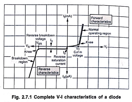
10. Draw the VI
characteristics of a PN junction diode.
11. Why a series resistor
is necessary when a diode is forward biased ?
For
limiting the forward current which increases exponentially with voltage.
12. What is meant by
breakdown voltage in PN junction diode ?
In
reverse biased condition, as reverse voltage increases the reverse current is
almost constant upto certain value of reverse voltage. At some reverse voltage,
the diode breaks down and large reverse current flows through it. The voltage
at which the diode breakdown occurs is called reverse breakdown voltage.
13. State the expression
for the dynamic resistance of a diode.
The
dynamic resistance of a diode is given by,
r = ηVT / I0eV/ηVT
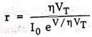
where
I0
= Reverse saturation current in amperes,
V
= Applied voltage,
VT
= Voltage equivalent of temperature in volts,
η = 1 for Ge diode and 2 for Si diode
14. What is p‒n junction
diode ?
The
two materials namely p‒type and n‒type are chemically combined with a special
fabrication technique to form p‒n junction. There are two electrodes each from
p‒type and n‒type materials and due to due to these two electrodes
(di+electrode), the device is called a diode. It conducts only in one
direction.
15. A silicon diode has a
saturation current of 7.5 μA at room temperature 300 °K. Calculate the
saturation current at 400 °K.
T1 = 300 °K, T2 = 400
°K, I01 = 7.5 μA, ΔT = T2‒ T1 = 100
I02 = (2ΔT/10) (I01)
=
2(100/10) × 7.5
=
7680 μA
=
7.68 mA
16. A Ge diode has a
saturation current of 10 μА at 300 °K. Find the saturation current at 400 °K.
T1= 300 °K,
T2
= 400 °K,
I01
= 10 μA
i.e.
ΔT = T2‒T1=100
I02 = (2ΔT/10) I01
=
(2100/10) × 10×10‒6
=
10.24 mA
17. What is is avalanche
breakdown ?
When
reverse voltage is increased, the velocity of minority charge carriers
increases. In such highly accelerated charge carrier collides against electron
involved in covalent bond, then it breaks the covalent bond and creats new
electron‒hole pair. These secondary particles also accelerate and involve in
the further collisions to produce more electron‒hole pairs. This is called
carrier multiplication. Due to such large number of charge carriers breakdown
of junction takes place. Such a breakdown is called avalanche breakdown.
18. Define storage time.
When
the diode is switched from forward biased to reverse biased, the minority
charge carriers remain stored and decrease slowly to zero. This time for which
minority charge carriers remain stored is called storage time.
19. Define transition time.
The
time required by the diode current to reduce to its reverse saturation value,
after minority carrier concentration reduces to zero is called transition time.
20. Define reverse recovery
time.
The
total time required by a diode to switch from ON to OFF state which is addition
of storage time and transition time is called reverse recovery time of a diode.
Trr
= ts + tt
21. What is the principle
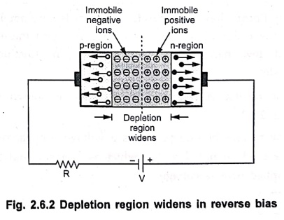
operation of a PN Junction diode in reverse bias condition ?
• When the p‒n junction is reverse biased the negative terminal attracts the holes in the p‒region, away from the junction.
• The positive terminal attracts the free electrons in the n‒region away from the junction.
• No charge carrier is able to cross the junction.
• As electrons and holes both move away from the junction, the depletion region widens.
• This creates more positive ions and hence more positive charge in the n‒region and more negative ions and hence more negative charge in the n‒region. This is because the applied voltage helps the barrier potential. This is shown in Fig. 2.6.2.
22. Sketch the forward bias
characteristics of the pn Junction dlode.
23. What are the applications
of PN diode ?
The
various applications of p‒n diode are, different types of rectifiers, various
protection circuits, multivibrators, in amplitude limiting circuits for
oscillators, clipper circuits, clamper circuits, in various electronic and op‒amp
based circuits, comparators. schemitt trigger circuits etc.
24. Find the voltage at
which the reverse current in a germanium PN junction diode attains a value of
90% of its saturation value at room temperature.
η = 1 for Ge,
VT
= 26 mV at room temperature
I
= 0.9 I0 but reverse hence take negative
I
= I0 [eV/nVT ‒1]
‒0.9
I0 = I0[eV/26×10‒3
‒1]
‒0.91 + 1 = e V/26×10‒3
i.e.
In 0.1 = V / 26×10‒3
V
= 2.3026×26×10‒3 = ‒59.867 mV
The
negative sign indicates the reverse voltage applied to the diode.
25. State the relationship
between diffusion capacitance and diode current in a PN diode.
The
diffusion capacitance is given by,
CD
= τI / ηVT
where
I is the diode current.
26. Determine the total
forward bias current density in a PN junction diode under an applied forward
bias voltage of 0.65 V at 300 K.
Assume JS = 4.155
× 10‒11 A/cm2.
V=
0.65 V, T = 300 °K,
JS
= 4.155×10‒11 A/cm2
The
diode current equation is,
I = IS[eV/ηVт −1]
...Divided by area
VT
= 26 mV at 300 °K, η = 1
J
= 4.155×10‒11 [e0.65/26x10‒3 ‒1]
J
= 3 A/cm2
……. Forward bias current density
27. Define diffusion
capacitance.
In
forward bias condition, the width of depletion region decreases and more holes
on p‒side get diffused in n‒side while electrons from n‒side move into p‒side.
As the applied voltage increases, the concentration of the injected charged
particles increases. This rate of change of the injected charge with the
applied voltage is defined as diffusion capacitance.
Electron Devices: Chapter 2: PN Junction Diodes : Tag: electronics : Electron Devices - PN Junction Diodes: Two Marks Important Questions and Answers
Electron Devices: Chapter 2: PN Junction Diodes
Under Subject

Electron Devices
EC25C01 2nd Semester ECE Dept | 2025 Regulation | 2nd Semester 2025 Regulation
Related Subjects

English Essentials II
EN25C02 2nd Semester | 2025 Regulation | 2nd Semester 2025 Regulation

Tamils and Technology தமிழர்களும் தொழில்நுட்பமும்
UC25H02 2nd Semester | 2025 Regulation | 2nd Semester 2025 Regulation

Linear Algebra
MA25C02 2nd Semester | 2025 Regulation
Electron Devices
EC25C01 2nd Semester ECE Dept | 2025 Regulation | 2nd Semester 2025 Regulation

Data Structures using CPlusPlus
CS25C05 2nd Semester ECE Dept | 2025 Regulation | 2nd Semester 2025 Regulation

Circuits and Network Analysis
EC25C02 2nd Semester ECE Dept | 2025 Regulation | 2nd Semester 2025 Regulation

Re-Engineering for Innovation
ME25C05 2nd Semester | 2025 Regulation | 2nd Semester 2025 Regulation

Engineering Drawing - Laboratory
ME25C01 2nd Semester | 2025 Regulation | 2nd Semester 2025 Regulation

Data Structures using CPlusPlus - Laboratory
CS25C05 2nd Semester ECE Dept | 2025 Regulation | 2nd Semester 2025 Regulation

Devices and Circuits Laboratory
EC25C03 2nd Semester ECE Dept | 2025 Regulation | 2nd Semester 2025 Regulation