Electron Devices: Chapter 2: PN Junction Diodes
Diffusion Capacitance of PN Junction Diode
Questions: 1. Explain the concept of diffusion capacitance of a p‒n junction diode. 2. Derive the expression for the diffusion capacitance of p‒n junction diode.
Diffusion
Capacitance (CD)
•
During forward biased condition, an another capacitance comes into existence
called diffusion capacitance or storage capacitance, denoted as CD.
•
In forward biased condition, the width of the depletion region decreases and
holes from p side get diffused in n side while electrons from n side move into
the p‒side.
•
As the applied voltage increases, concentration of injected charged particles
increases.
•
This rate of change of the injected charge with applied voltage is defined as a
capacitance called diffusion capacitance.
CD = dQ / dV
……. (2.14.1)
•
The diffusion capacitance can be determined by the expression
CD = τI / ηVT
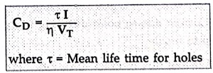
... (2.14.2)
•
So diffusion capacitance is proportional to the current.
•
For forward biased condition, the value of diffusion capacitance is of the
order of nano farads to micro farads while transition capacitance is of the
order of pico farads. So CD is much larger than CT.
•
However in forward biased condition, CD appears in parallel with the
forward resistance which is very very small. Hence the time constant which is
function of product of the forward resistance and CD is also very
small for ordinary signals.
Key
Point: For normal signals CD has no practical
significance but for fast signals CD must be considered.
•
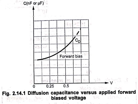
The graph of CD against the applied forward voltage is shown in Fig.
2.14.1.
•
As applied forward voltage increases, current I increases hence diffusion
capacitance CD increases.
Derivation of Expression for Diffusion Capacitance
•
In a p‒n junction the total current at the junction (x = 0) is given by,
I = Ipn(0) + Inp(0)A
where
Ipn(0)
= Current due to holes diffusing from p to n side
Inp(0)
= Current due to holes diffusion from n to p side
•
Let p side is heavily doped with respect to other hence Inp(0) is
negligible compared to Ipn(0).
I = Inp(0)
•
The diffusion current density is given by,
Jp(x) = ‒q Dp (dpn/dx)
where
Dp
= Diffusion constant
dpn/dx
= Concentration gradient
•
Also
J
= Current / Area = I/A
i.e.
Ip(x) = Jp(x) A
Ip(x)
= ‒q A Dp (dpn/dx)
...(2.14.3)
•
For a p‒n junction,
Pn(x) = Pn (0) e‒x/Lp
...(2.14.4)
where
Lp
= Diffusion length for holes
•
From equation (2.14.4) Dpn (x)/dx = Pn(0) e‒x/Lp
(‒1/Lp)
Ip(x) = ‒ q A Dp Pn(0)
e‒x/Lp (‒1/Lp)
Ip(x) = q A (Dp/Lp) Pn(0)
e‒x/Lp
•
At x = 0, Ip(x) = Ipn(0) = I
i.e.
I = qADpPn(0) / Lp
...(2.14.5)
Pn(0)
= ILp / qADp
...(2.14.6)
•
The excess minority charge Q exists only on n side and given by,
Q
= 0∫∞ AqPn(0) e‒x/Lp dx
= [AqPn(0) ( e‒x/Lp /
‒1/Lp ) ]0∞
=
AqLpPn(0)
...(2.14.7)
Using
equations (2.14.6) in (2.14.7)
Q = AqLpILp / qADp
= Lp2I / Dp
...(2.14.8)
•
But L2/Dp = τ = Mean life time of charge carriers.
Q = τI
and
CD = dQ/dV = dQ/dl . dl/dV
•
But dQ/dI = τ hence CD = τ dI/dV
•
From diode current equation,
I = I0 eV/ηVT
…………… Neglecting 1 from equation
dI/dV
= I0 eV/ηVT
. 1/ ηVT
= 1 / ηVT
….....(2.14.10)
CD = τI / ηVT = Diffusion capacitance
Review
Questions
1. Explain the concept of diffusion capacitance of a p‒n
junction diode.
2. Derive the expression for the diffusion capacitance of p‒n
junction diode.
Electron Devices: Chapter 2: PN Junction Diodes : Tag: electronics : - Diffusion Capacitance of PN Junction Diode
Electron Devices: Chapter 2: PN Junction Diodes
Under Subject

Electron Devices
EC25C01 2nd Semester ECE Dept | 2025 Regulation | 2nd Semester 2025 Regulation
Related Subjects

English Essentials II
EN25C02 2nd Semester | 2025 Regulation | 2nd Semester 2025 Regulation

Tamils and Technology தமிழர்களும் தொழில்நுட்பமும்
UC25H02 2nd Semester | 2025 Regulation | 2nd Semester 2025 Regulation

Linear Algebra
MA25C02 2nd Semester | 2025 Regulation
Electron Devices
EC25C01 2nd Semester ECE Dept | 2025 Regulation | 2nd Semester 2025 Regulation

Data Structures using CPlusPlus
CS25C05 2nd Semester ECE Dept | 2025 Regulation | 2nd Semester 2025 Regulation

Circuits and Network Analysis
EC25C02 2nd Semester ECE Dept | 2025 Regulation | 2nd Semester 2025 Regulation

Re-Engineering for Innovation
ME25C05 2nd Semester | 2025 Regulation | 2nd Semester 2025 Regulation

Engineering Drawing - Laboratory
ME25C01 2nd Semester | 2025 Regulation | 2nd Semester 2025 Regulation

Data Structures using CPlusPlus - Laboratory
CS25C05 2nd Semester ECE Dept | 2025 Regulation | 2nd Semester 2025 Regulation

Devices and Circuits Laboratory
EC25C03 2nd Semester ECE Dept | 2025 Regulation | 2nd Semester 2025 Regulation